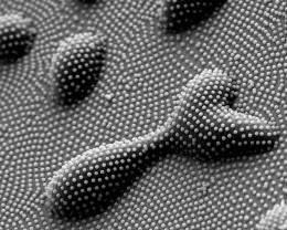
Polymer scientists make imprint on nanolithography

(PhysOrg.com) -- Nanolithography, or surface patterning on a nanoscale, is critical for modern technology, but has been developed largely for patterning flat surfaces until recently. A team of University of Akron scientists discovered a new method for patterning curved surfaces. The technique creates patterns on curved or topographically uneven surfaces with stand-alone nanoparticles, opening new technology opportunities.
Findings by University of Akron graduate students Sarang P. Bhawalkar, Jun Qian (a visiting student from Tianjin University, China), Michael C. Heiber, and assistant professor of polymer science Dr. Li Jia are available in the Nov. 16, 2010 issue of Langmuir, a publication of the American Chemical Society.
“Nanoparticles arranged in hexagonal patterns have been widely used for surface patterning before our work, but these particles touch and support each other,” explains Jia. “We were curious to learn if we could use stand-alone particles not supporting each other. There are several advantages to this. Among them is the possibility of patterning curved or uneven surfaces. Consider traditional photolithography, which is highly efficient in putting complex circuits on flat computer chips, but inapt at patterning surfaces that are not flat.”
The challenge, according to Jia, was to secure the pattern against the lateral capillary force. When this challenge was presented to Sarang, his solution was to dip-coat a layer of polymer adhesive.
“It worked like a charm,” Jia says.
According to Jia, the method is a breakthrough due to adaptation to topographic features ranging from macroscopic to microscopic scales. The team is currently working on fabrication of surfaces with a combination of several advanced properties such as self-cleaning, anti-reflection and anti-icing, says Jia, who notes the desirability of these surface properties in skyscrapers, aircrafts, solar panels and residential windows.
The researchers are testing their lithography method on large surfaces and durability of the patterns when subjected to temperature fluctuations and abrasion. Jia adds that he and his colleagues’ next step, in collaboration with other experts, is to explore the applications of their lithography method in optical circuitry, imaging and sensing, and bioengineering.
More information: See “Development of a Colloidal Lithography Method for Patterning Nonplanar Surfaces” at pubs.acs.org/doi/abs/10.1021/la1035147
Provided by University of Akron


