Microtechnology: An alignment assignment

Microelectromechanical systems (MEMS), which consist of tiny moving parts driven by electrical signals, have found ready applications in optical communication systems. They are attractive in part because they can be integrated with other electrical and optical components to create a multifunctional device in a single package, which reduces fabrication costs and allows for greater performance. However, this integration requires precise alignment of the constituent parts in order to avoid signal loss.
One approach to achieve accurate alignment is to manufacture both the optical MEMS components and any other electronic or photonic components on the same silicon wafer. Optical MEMS devices, however, are often ten times thicker than other optical components. This means that different fabrication techniques are needed for the different components, making alignment difficult.
Another approach is to fabricate MEMS and electrical components on two separate wafers that are then bonded together. Achieving good alignment in this scheme is made difficult, however, by the coarse bonding processes that are available. Qingxin Zhang and co-workers at the A*STAR Institute of Microelectronics have now refined the two-wafer approach by combining the final fabrication step for each component into a single process.
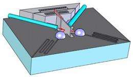
The research team aligned an optical MEMS structure with a silicon photonic structure (see figure). The two wafers bearing the respective components were processed independently in the first step: the MEMS structure was fabricated on a bulk silicon wafer and the photonic structure on a silicon-on-insulator wafer. The wafers were then bonded together using benzocyclobutene—a commonly used bonding agent for MEMS—at 250 °C, and the two structures were completed simultaneously using a single step of deep reactive ion etching.
The use of a single fabrication step to complete the final integrated device allowed Zhang and his co-workers to meet strict alignment specifications, achieving a misalignment of less than one micrometer laterally and less than half a micrometer vertically. They also used their strategy to construct and characterize a functioning optical switch in which a MEMS mirror is displaced by a driving voltage to connect and disconnect an optical pathway. The signal loss between a source optical fiber and the silicon waveguide in the device was just 2.4 decibels, which is well within acceptable limits.
The new approach allows scientists to merge photonic and MEMS components fabricated on two different wafers into a single device. Future work will focus on optimizing the MEMS design and fabrication process, and demonstrating reconfigurability.
More information: Zhang, Q. et al. A two-wafer approach for integration of optical MEMS and photonics on silicon substrate. IEEE Photonics Technology Letters 22, 269–271 (2010).
Provided by Agency for Science, Technology and Research (A*STAR)


