January 24, 2011 feature
Solving the solar cell power conversion dilemma

(PhysOrg.com) -- "There is a lot of interest in creating more efficient solar cells that are also simpler than many of the designs common now," Wladek Walukiewicz tells PhysOrg.com. "We think that, through the mixing of certain semiconductors, this is possible."
Walukiewicz has lead a group of scientists working at the Lawrence Berkeley National Laboratory, Rose Street Labs Energy and Sumika Electronic Materials, Inc. They have been studying the properties of GaNAs alloys, and they believe that the characteristics of these semiconductor alloys could lead to more efficient solar cells. Their work appears in Physical Review Letters: "Engineering the Electronic Band Structure for Multiband Solar Cells."
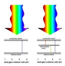
"In solar cells made of standard semiconductors, the electric current is produced by electron-hole pairs photo-excited across the band gap separating the conduction and the valence band," Walukiewicz explains. "Only the photons with the energy larger than the band gap can produce electric current. This creates the solar cell power conversion dilemma."
This dilemma is occurs when "a small gap semiconductor absorbs more photons and produces larger current but small voltage whereas a large gap semiconductor produces larger voltage but the current is limited because large fraction of the solar photons is not absorbed," he continues. "However, there is a gap between these bands, with no state. Normally, this doesn't conduct. Exciting a semiconductor with light can help, though."
This dilemma means that in order for a solar cell device to be efficient, it must be complex, incorporating different layers with different gaps so that different portions of the solar spectrum can be absorbed. “Silicon solar cells are only up to20% efficient,” Walukiewicz says. “There are those that are as much as 40% efficient, but they are so complex – and expensive.”
Walukiewicz and his colleagues believe that they have found a way around this. By using GaNAs alloys, the group has created a single material that can absorb multiple portions of the solar spectrum. “Scientists have been mixing semiconductors for years, creating materials with properties tailored for specific applications.” Walukiewicz says. “But they were working with semiconductors that wanted to be mixed. We work with materials that don’t want to be mixed, using special methods to force them.”

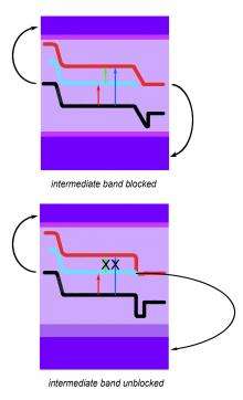
When this mixing happens, Walukiewicz points out, interesting properties are seen, like the one that allows for an intermediate band of states to be formed in a wide gap semiconductor. The band acts as a stepping stone in the semiconductor band gap. “Our device is quite simple,” he says. “For years, people have been creating efficient solar cells using many semiconductors with different gaps. We have developed a semiconductor built with multiple bands.”
As a result, solar cells developed with the GaNAs alloys have the potential to contribute to solving a problem in the world of solar energy. “We don’t know exactly what to expect, but we estimate that a solar cell made as we describe would be more than 40% efficient,” Walukiewicz says. “However, it would be much less complex than what is used now to do the same thing. Right now, it is common for 18 layers of semiconductors to be used to reach that level of efficiency. Our technique could possibly do it with four or five layers.”
Such a device could be much easier to make, and could possibly be scalable for production for a wider market. It would also likely be more cost efficient. “Our objective is to develop it to a point where it would be commercially viable, and even make a difference.”
More information: N. López, L.A. Reichertz, K.M. Yu, K. Campman, and W. Walukiewicz, “Engineering the Electronic Band Structure for Multiband Solar Cells,” Physical Review Letters (2011). Available online: link.aps.org/doi/10.1103/PhysRevLett.106.028701
Copyright 2010 PhysOrg.com.
All rights reserved. This material may not be published, broadcast, rewritten or redistributed in whole or part without the express written permission of PhysOrg.com.


