New technique boosts high-power potential for gallium nitride electronics

Gallium nitride (GaN) material holds promise for emerging high-power devices that are more energy efficient than existing technologies – but these GaN devices traditionally break down when exposed to high voltages. Now researchers at North Carolina State University have solved the problem, introducing a buffer that allows the GaN devices to handle 10 times greater power.
"For future renewable technologies, such as the smart grid or electric cars, we need high-power semiconductor devices," says Merve Ozbek, a Ph.D. student at NC State and author of a paper describing the research. "And power-handling capacity is important for the development of those devices."
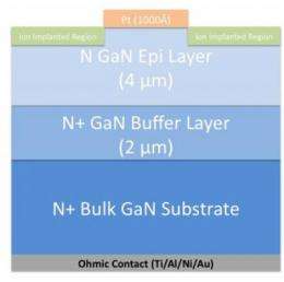
Previous research into developing high power GaN devices ran into obstacles, because large electric fields were created at specific points on the devices' edge when high voltages were applied – effectively destroying the devices. NC State researchers have addressed the problem by implanting a buffer made of the element argon at the edges of GaN devices. The buffer spreads out the electric field, allowing the device to handle much higher voltages.
The researchers tested the new technique on Schottky diodes – common electronic components – and found that the argon implant allowed the GaN diodes to handle almost seven times higher voltages. The diodes that did not have the argon implant broke down when exposed to approximately 250 volts. The diodes with the argon implant could handle up to 1,650 volts before breaking down.
"By improving the breakdown voltage from 250 volts to 1,650 volts, we can reduce the electrical resistance of these devices a hundredfold," says Dr. Jay Baliga, Distinguished University Professor of Electrical and Computer Engineering at NC State and co-author of the paper. "That reduction in resistance means that these devices can handle ten times as much power."
More information: The paper, "Planar, Nearly Ideal Edge Termination Technique for GaN Devices," is forthcoming from IEEE's Electron Device Letters.
Provided by North Carolina State University


