Major advance in understanding how nanowires form

New insights into why and how nanowires take the form they do will have profound implications for the development of future electronic components. PhD student Peter Krogstrup from the Nano-Science Center at the Niels Bohr Institute, University of Copenhagen is behind the sensational new theoretical model, which is developed in collaboration with researchers from CINAM-CNRS in Marseille. The results have been published in the scientific magazine, Physical Review Letters.
One of the most important components in future electronic devices will likely be based on nanocrystals, which are smaller than the wavelength of the light our eyes can detect. Nanowires, which are extremely thin nanocrystal wires, are predicted to have a predominant role in these technologies because of their unique electrical and optical properties. Researchers around the world have been working for years to improve the properties of these nanowires.
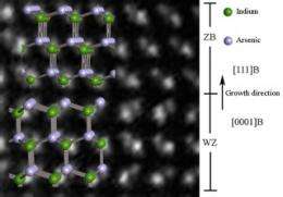
With his research, PhD student Peter Krogstrup at the Niels Bohr Institute, University of Copenhagen has laid the foundations for a greater understanding of nanowires. With that comes the potential for improving their performance, which will bring the research closer to being applied in the development of solar cells and computers. In the latest edition of Physical Review Letters he describes how, under certain conditions, nanowires form a crystal structure that really should not be possible, seen from an energy perspective.
"Crystals will always try to take the form in which their internal energy is as little as possible. It is a basic law of physics and according to it these nanowires should have a cubic crystal structure, but we almost always see that a large part of the structure is hexagonal", explains Peter Krogstrup, who has been working with the theory in recent years.
Catalyst particle shape is the key
In order to explain why and when these crystals become hexagonal, Peter Krogstrup has, as part of his doctoral dissertation, examined the shape of the catalyst particle (a little nano-droplet), which controls the growth of the nanowires. It appears that the shape of the droplet depends on the amount of atoms from group 3 in the periodic system, which make up half of the atoms in the nanowire crystal. The other half, atoms from group 5 in the periodic system, are absorbed by the drop and hence the atoms organize themselves into a lattice, and the nanowire crystal will grow.
"We have shown that it is the shape of the droplet, which determines what kind of crystal structure the nanowires obtain and with this knowledge it will be easier to improve the properties of the nanowires", explains Peter Krogstrup and continues:
"The crystal structure has an enormous influence on the electrical and optical properties of the nanowires and you would typically want them to have a certain structure, either cubic or hexagonal. The better nanowires we can make the better electronic components we can make to the benefit of us all", says Peter Krogstrup, whose research is conducted in collaboration with the firm SunFlake A/S, which is located at the Nano-Science Center at the Niels Bohr Institute, University of Copenhagen. The company is working to develop solar cells of the future based on nanowires.
More information: prl.aps.org/abstract/PRL/v106/i12/e125505
Provided by Niels Bohr Institute


