March 21, 2011 feature
Transistor performance improves due to quantum confinement effects

(PhysOrg.com) -- Manufacturing on the nanoscale has come a long way since Feynman’s visions of nanotechnology more than 50 years ago. Since then, studies have demonstrated how low-dimensional structures, such as nanowires and quantum dots, have unique properties that can improve the performance of a variety of devices. In the latest study in this area, researchers have fabricated transistors made with exceptionally thin silicon nanowires that exhibit high performance due to quantum confinement effects in the nanowires.
The team of researchers, Krutarth Trivedi, Hyungsang Yuk, Herman Carlo Floresca, Moon J. Kim, and Walter Hu, from the University of Texas at Dallas, has published their study in a recent issue of Nano Letters.
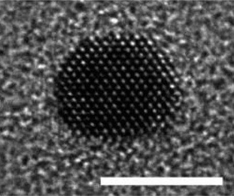
In their study, the researchers lithographically fabricated silicon nanowires with diameters of just 3-5 nanometers. With a diameter this small, the nanowires experience quantum confinement effects that cause the nanowires’ properties to change from their bulk values. Specifically, transistors made with the thin nanowires have improved hole mobility, drive current, and current density – properties that make the transistors operate more quickly and efficiently. The transistors’ performance even surpasses recently reported silicon nanowire transistors that use doping to improve their performance.
“The significance of this research is that we have demonstrated that increasing the degree of quantum confinement of the silicon channel results in increasing the carrier mobility,” Hu told PhysOrg.com. “We provide experimental proof of the theoretically simulated high hole mobility of about 3-nm-diameter nanowires.”
At first, it may seem counterintuitive that a smaller wire can have a higher mobility than a larger wire. But as the researchers explain, quantum confinement effects increase carrier mobility in the wire by confining the holes (which contribute to the current) to a more uniform range of energy than they have in bulk silicon. Whereas in bulk silicon, holes having a broad energy distribution contribute to the current, in the tiny nanowires, the energy of the holes has a much narrower distribution. Having holes with similar energy, and therefore mass, reduces carrier scattering effects in the nanowires, which in turn improves mobility and current density. By comparing the performance of tiny nanowires to similarly fabricated nanobelts, in which only the thickness dimension is confined, the researchers also show that increasing the degree of quantum confinement of the channel results in higher carrier mobility.
As the researchers note, fabricating the high-performance sub-5-nanometer silicon nanowire transistors is relatively simple compared to other methods of nanowire fabrication, which use bottom-up methods and doped junctions or channel doping. One application that the researchers plan to pursue is using the nanowires to make inexpensive, ultrasensitive biosensors, since biosensor sensitivity increases as nanowire diameter decreases.
“As required by our funding (NSF Career Award), our immediate plan is to explore biosensing of protein with these types of tiny nanowire transistors,” Hu said. “We believe such small-diameter nanowires with intrinsic high performance can have a major impact on biosensing, as they are expected to provide ultimate sensitivity down to a single molecule with a better signal-to-noise ratio.”
In addition to biosensing, the new high-performance transistors could have an impact on CMOS scaling, which is becoming increasingly difficult. The researchers are currently looking for funding in order to explore this area.
“These transistors can have an impact on CMOS scaling due to the fact that performance actually increases with decreasing diameter,” Hu said. “Arrays of nanowire transistors with tiny nanowires could be made to achieve high performance without requiring new processing techniques. In fact, the processing can even be simplified over current techniques, as our nanowire transistors do not use highly doped complementary junctions for source/drain; eliminating high doped junctions alleviates many of the current issues in scaling down CMOS processing techniques to the nanoscale.
“At large, my personal viewpoint is that silicon still has a lot of potential for nanoelectronics, and the industry may want to consider supporting research in silicon nanowire or quantum wire devices and new architectures to fully unleash the potential of silicon. Everyone is researching graphene, which is a great material of course, but we may not want to ignore the potential of silicon, as we show that effective hole mobility can be over 1200.”
More information: Krutarth Trivedi, et al. “Quantum Confinement Induced Performance Enhancement in Sub-5-nm Lithographic Si Nanowire Transistors.” Nano Letters. DOI:10.1021/nl103278a
Copyright 2010 PhysOrg.com.
All rights reserved. This material may not be published, broadcast, rewritten or redistributed in whole or part without the express written permission of PhysOrg.com.


