Engineers create vibrant colors in vertical silicon nanowires

(PhysOrg.com) -- Engineers may soon be singing, "I'm going to wash that gray right out of my nanowires," thanks to a colorful discovery by a team of researchers from Harvard University and Zena Technologies. In contrast to the somber gray hue of silicon wafers, Kenneth B. Crozier and colleagues demonstrated that individual, vertical silicon nanowires can shine in all colors of the spectrum.
The vibrant display, dependent on the diameter of the individual wires, is even visible to the naked eye. In addition to adding a splash of color to the lab, the finding has potential for use in nanoscale image sensor devices, offering increased efficiency and the ability to detect color without the use of filters.
"It is surprising," says Crozier, John L. Loeb Associate Professor of the Natural Sciences at the Harvard School of Engineering and Applied Science (SEAS). "A lot of people are making nanowires, and you really don't think of the color so much. In this vertical configuration you can get very strong color effects, and you can tune them over a range of wavelengths of the visible region. The strong effects can be seen right down to the level of the individual wire."
The finding, published in the March 17, 2011, online edition of Nano Letters, may be the first experimental report that silicon nanowires can take on a variety of colors depending on their diameter and under bright-field illumination. Previous work has shown that nanowires can take on different colors but only by looking at scattered, rather than directly reflected, light.
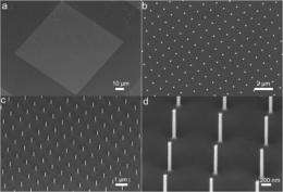
To create the multicolored array of vertical silicon nanowires, the engineers at Harvard and Zena Technologies used a combination of electron beam lithography and inductively coupled plasma reactive ion etching.
A smooth wafer of silicon was plasma etched until all that remained were the vertically protruding nanowires, resembling bristles on a toothbrush. While the nanowires were created in arrays of thousands for convenience, the colors they exhibited were due to the properties of the individual wires, not by the way light was scattered or diffracted in the group.

"Each nanowire acts as a waveguide, like a nano-sized optical fiber—but an optically absorbing one," explains Crozier. "At short wavelengths there is not much optical coupling to the nanowire. At long wavelengths, the coupling is better, but the properties of the waveguide are such that there is not much absorption. In between, there is a range of wavelengths where the light is coupled to the nanowire and absorbed. This range is determined by the nanowire diameter. We made nanowires with diameters of 90, 100, and 130 nm that appeared red, blue and green, respectively."
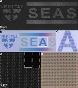
To demonstrate the remarkable phenomenon and the relative ease of controlling and positioning the colorful nanowires, the researchers created a nanoscale-sized tribute to Harvard, designing a pattern resembling the engineering school's Veritas seal and spelling out the acronym SEAS in a rainbow of colors.
While the Harvard image closely matched the school's seal, the desired color eluded the engineers.
"We actually wanted to make the seal red rather than blue, but it turned out that the diameter was a little bit wrong," says Crozier.
As even small changes in the radius of a wire can alter the color, the seal turned out to be blue, more suitable for the famous seal of a certain other Ivy League institution.
Fortunately, the technology has other promising applications. The researchers' eventual aim is to use the wires in image sensors. Traditional photodetectors in image sensor devices can gauge the intensity of light but not determine its color without the use of an additional filter, which throws away much of the light, limiting the device's sensitivity.
The researchers hope to address this by fabricating vertical nanowires containing photodetectors above standard photodetectors formed on a silicon wafer. The nanowire and standard photodetectors could each detect a different part of the spectrum of the incident light. By comparing the signals from each, the color could be determined without losing so much of the light.
"With image sensors, every little bit of efficiency counts. Moreover, we even imagine using the colored wires to encode data in a read-only type of information storage," adds Crozier.
Provided by Harvard University


