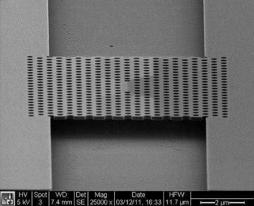
Stanford engineers create a tiny, energy-efficient laser for optical communication systems

(PhysOrg.com) -- In the push toward ever-smaller and ever-faster data transmission technology, a team of Stanford electrical engineers has produced a nanoscale laser that is much faster and vastly more energy efficient than anything available today.
To the Silicon Valley mantra of "faster, smaller" semiconductors, you can now add "more efficient." The electrical data interconnections inside the computers of America's massive datacenters consume huge amounts of electricity, and there is a technological drive afoot to reduce that consumption.
To that end, Stanford researchers have unveiled a tiny, highly efficient semiconductor laser that could herald a new era in low-energy data interconnects that communicate with light as well as electrons.
"Today's electrical data transmission circuits require a lot of energy to transmit a bit of information and are, relatively speaking, slow," said Jelena Vuckovic, an associate professor of electrical engineering at Stanford working on the new generation of nanoscale lasers.
She and her team – including Stanford graduate students Bryan Ellis and Gary Shambat, in collaboration with the research groups of James Harris at Stanford and Eugene Haller at the University of California-Berkeley – introduced their laser in a paper just published in Nature Photonics.
Crossing the threshold
Vuckovic is working on a type of data transmitter known as a photonic-crystal laser. These lasers are particularly promising, not just for their speed and size, but because they operate at low thresholds – they don't use much energy.
"We've produced a nanoscale optical data transmitter – a laser – that uses 1,000 times less energy and is 10 times faster than the very best laser technologies in commercial use today," said the professor. "Better yet, we believe we can improve upon those numbers."
While others have created low-threshold lasers, Vuckovic said, the most promising have required a second laser to inject them with the energy they need to work – known as "pumping" – hardly an ideal solution.
"We really needed a laser pumped with electricity, not light," she said. The only available electrically pumped photonic-crystal laser was inefficient and difficult to fabricate, making it commercially impractical. Now, for the first time, Vuckovic has demonstrated an electrically pumped laser that is both easy to manufacture and delivers dramatically reduced energy consumption.
To create the laser, the researchers first "grow" a wafer of gallium arsenide, a semiconductor crystal, using a beam that sprays molecules to build layers one by one. At certain points in the layering process, they shuffle in three thin layers of a second crystal – indium arsenide. A cross-section reveals that the indium arsenide appears like little bumps or hills – quantum dots – within the wafer.
A deck of cards
When done, the wafer resembles a sort of nanophotonic deck of cards a mere 220 nanometers thick. Thick, however, is a relative term. It would take more than 1,000 of Vuckovic's wafers stacked atop one another to equal the thickness of a single playing card.
Next, the engineers "dope" two discrete areas on top of the wafer with ions. On one side, the researchers seed ions of silicon, and on the other they implant ions of beryllium.
These two regions are faintly visible on the surface, widening toward each other, approaching but never quite meeting at the center of the wafer. These ion-infused regions help focus the current flow to a very precise area at the core of the wafer where light is emitted, improving the performance of the laser.
Finally, with the basic wafer fabricated, the researchers have yet one more trick up their engineering sleeves. They finish by etching a precise honeycomb pattern of circular holes through the wafer.
The size and positioning of these holes is critical to the success of the laser. If the holes are too small or too large, spaced too closely or too far apart, the laser will not perform optimally – in some cases, it won't perform at all.
"These holes are almost perfectly round with smooth interior walls and are very important to the laser's function. They act like a hall of mirrors to reflect photons back toward the center of the laser," said Vuckovic.
Here, in the heart of the wafer, the photons are concentrated and amplified into a tiny ball of light – a laser – which can be modulated up to 100 billion times per second, 10 times the best data transmitters now in use. Thus the light becomes binary data – light on, 1; light off, 0.
Real-world possibilities
At one end of a semiconductor circuit is a laser transmitter beaming out 1s and 0s as blasts of light. At the other end is a receiver that turns those blasts of light back into electrical impulses. All that is needed is a way to connect the two.
To do this, the researchers heat and stretch a thin fiberoptic filament, hundreds of times thinner than a human hair. The light from the laser travels along the fiber to the next junction in the circuit.
All this happens in a layer so thin hundreds of these nanophotonic transmitters could be arranged on a single layer, and many layers could then be stacked into a single chip.
Before Vuckovic's laser interconnect becomes commonplace, however, certain questions will need to be resolved. The new laser operates at relatively cold temperatures, 150 degrees Kelvin and below – about 190 degrees below zero Fahrenheit – but Vuckovic is confident and pressing forward.
"With improvements in processing," she said, "we can produce a laser that operates at room temperature while maintaining energy efficiency at about 1,000 times less than today's commercial technologies. We can see a light on the horizon."
Provided by Stanford University


