June 14, 2011 feature
Lighten up: Polaritons with tunable photon-exciton coherence

(PhysOrg.com) -- Of the many exotic and counterintuitive aspects of particle and quantum physics, exciton and polariton quasiparticles are among the most interesting. An exciton forms when a photon is absorbed by a semiconductor as a Coulomb force-bound state of a (negatively-charged) electron and a (positively-charged) hole; this particle pair can be seen as an elementary excitation of condensed matter able to transport energy without the transfer of net electric charge, and moreover has size- and shape-dependent optoelectronic properties. A polariton forms due to strong coupling of a photon with an excitation of a material – and among the several types of polaritons, an exciton-polariton is a composite photonic-electronic quasiparticle resulting from coupling of visible light with matter in the form of an exciton. At the same time, the difficulty of achieving increased light-matter coupling strengths has limited the development of applications operating at, for example, higher temperatures and lower power. Recently, however, researchers produced light-matter coupling strengths in nanoscale materials at much higher levels than was previously thought possible in their bulk counterparts.
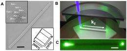
The research, conducted by Prof. Ritesh Agarwal and his team at the University of Pennsylvania, eschews the standard approach of working with electronically confined excitons inside two- or three- dimensional high reflectivity optical cavities in favor of one-dimensional cavity-polaritons, which they achieved using cadmium sulfide (CdS) nanowire waveguides. This dramatically increased light-matter coupling strength to levels far beyond those attainable in bulk materials with previous methods. Moreover, their success promises significant improvements in a wide range of areas, including low-threshold lasing; solid-state Bose-Einstein condensation; and sensing, switching and other slow-light applications.
In their efforts to discover and quantify that semiconductor crystals of sizes in between quantum dots (<~20nm) and bulk crystals (>~500nm) can exhibit enhanced and size-dependent light-matter coupling strengths, the team faced a number of obstacles. ”Information about the strength of the light-matter coupling is traditionally obtained by angle resolved measurements of the light dispersion inside the structure,” Agarwal explains. “However, due to the size on the order of the wavelength of light of the presently investigated crystals, this information is scrambled by diffraction and scattering, making the light dispersion inaccessible. Furthermore, for strong light-matter coupling to occur we need to pair up the excitations in the crystal into electron-hole pairs – a process which becomes more difficult with smaller crystals due to their larger surface-to-volume ratios. This causes relatively more competitive relaxation channels to form on the surface, which in turn ultimately diminishes the light-matter coupling strength.”
Typically, strong light-matter coupling is obtained by creating micropillars made by cutting a small chunk of the semiconductor crystal by wet or dry etching, which makes the surface very rough where excitons can get trapped, imposing a lower limit to the cavity size and thus a higher limit on the achievable coupling strength. However, Agarwal’s team circumvented this size problem by utilizing self-assembled semiconductor nanowire optical cavities which have dimensions on the order of the wavelength of light. “It was known that semiconductor nanowires can form length-wise standing optical wave cavities,” notes Agarwal. “We synthesized high optical quality semiconductor nanowires with widths down to 130 nm, used the standing wave energies to reconstruct the photon wave vectors, and subsequently fitted our theoretical model to the data to precisely extract the actual light-matter coupling strength.”
Going forward, Agarwal notes that while his team has clearly observed a dramatic increase in light-matter coupling strengths with respect to bulk materials, practical exploitation of potential benefits such as truly reduced power requirements for light manipulation is difficult to achieve using their current experimental setup. “In order to obtain measurable gains,” says Agarwal, “in- and out-coupling losses will have to be reduced by accessing nanowires using local components, ideally as part of an on-chip nanowire optical network.” When compared with the current system, this will reduce absolute power loss between an active nanowire switch and a nearby nanowire laser.
Agarwal sees a range of benefits from their new approach. In the near term, he notes, “exploitation of strong light-matter coupling strength could aid in reducing power requirements of simple signal routing within optical layers of hybrid optical/electronic chips1. Further down the line, precise manipulation of coupling strengths could potentially be used to perform logic operations using the nanowires themselves as active components in all-optical circuits.” Increased light-matter coupling strength is also important to fabricate so-called thresholdless polariton lasers, optical switches, modulators, routers and other photon integrated circuit components with smaller footprints and higher performance.
Especially enticing is Agarwal’s view of the potential for in vitro sensing applications made possible by the minute size (1000x thinner than human hair) of, and the reduced light velocity associated with enhanced light-matter coupling strength in, the nanowires. “They can act as highly miniaturized active waveguides for optical sensing with high spatial resolution,” he foresees. “The slowed light will lead to increased detection sensitivity due to the longer interaction time with the analytes.”
More information:
• One-dimensional polaritons with size-tunable and enhanced coupling strengths in semiconductor nanowires, PNAS, Published online before print, May 31, 2011, doi:10.1073/pnas.1102212108
• Agarwal Group at the University of Pennsylvania’s Department of Materials Science and Engineering
• 1IBM's breakthrough chip technology lights the path to exascale computing
Copyright 2011 PhysOrg.com.
All rights reserved. This material may not be published, broadcast, rewritten or redistributed in whole or part without the express written permission of PhysOrg.com.


