July 20, 2011 report
Japanese researchers develop method for printing single crystal thin-film transistors
(PhysOrg.com) -- Researchers working out of the National Institute of Advanced Industrial Science and Technology (AIST) in Tsukuba, Japan have developed a means for printing thin film transistors using InkJet technology. The team describes the process in their paper published in Nature.
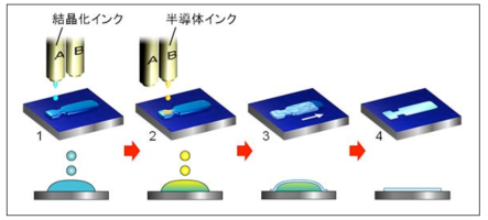
To get around the problem of self-crystallization, inherent in other InkJet/transistor making processes, which result in spreading effects that make it difficult to print uniformly, the team instead chose to use a two step process, whereby one type of ink is sprayed first onto a substrate and is then followed by another immediately afterwards, directly on top of the first; the two then mix, creating an environment whereby one single crisp and sharp crystal grows and adheres to the material it is printed on.
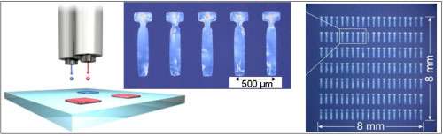
The first ink applied is a liquid (anhydrous dimethylformamide) that holds a semiconductor but is not soluble. The second is comprised of an organic semiconductor in a solvent. After the first is sprayed onto the substrate, followed by a shot of the second, the two then mix naturally, and then, from a single point in the mixture a tiny crystal begins to grow, and keeps on growing until the entire pool of ink is consumed, resulting in a thin film (30-200nm thick) of C8BTBT affixed to the substrate. After printing a complete pattern with their new process onto a substrate, other components were added to complete the transistor.
Researchers are looking at InkJet sprayed transistor technologies in the hope that it could lead to a whole host of products that are based on bendable substrates, such as flexible displays, solar cells, large sheets of sensors, or true ePaper, and because it would offer a lowered cost of production compared to traditional silicon based products.
The authors say their new method offers exceptionally uniform creation of the crystals, a development that could lead InkJet sprayed technology out of the lab and into real world products. The team next plans to look into whether their new technique could also be used to create metal wires which would allow for a transistor to be made entirely from InkJet spraying technology.
More information: Inkjet printing of single-crystal films, Nature (2011) doi:10.1038/nature10313
Abstract
The use of single crystals has been fundamental to the development of semiconductor microelectronics and solid-state science. Whether based on inorganic or organic materials, the devices that show the highest performance rely on single-crystal interfaces, with their nearly perfect translational symmetry and exceptionally high chemical purity. Attention has recently been focused on developing simple ways of producing electronic devices by means of printing technologies. ‘Printed electronics’ is being explored for the manufacture of large-area and flexible electronic devices by the patterned application of functional inks containing soluble or dispersed semiconducting materials. However, because of the strong self-organizing tendency of the deposited materials12, 13, the production of semiconducting thin films of high crystallinity (indispensable for realizing high carrier mobility) may be incompatible with conventional printing processes. Here we develop a method that combines the technique of antisolvent crystallization14 with inkjet printing to produce organic semiconducting thin films of high crystallinity. Specifically, we show that mixing fine droplets of an antisolvent and a solution of an active semiconducting component within a confined area on an amorphous substrate can trigger the controlled formation of exceptionally uniform single-crystal or polycrystalline thin films that grow at the liquid–air interfaces. Using this approach, we have printed single crystals of the organic semiconductor 2,7-dioctyl[1]benzothieno[3,2-b][1]benzothiophene (C8-BTBT), yielding thin-film transistors with average carrier mobilities as high as 16.4 cm2 V−1 s−1. This printing technique constitutes a major step towards the use of high-performance single-crystal semiconductor devices for large-area and flexible electronics applications.
AIST press release
© 2010 PhysOrg.com


