September 2, 2011 feature
Organic electronic devices could be printed on ordinary CDs and DVDs

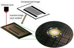
(PhysOrg.com) -- Organic electronics – those that involve carbon-based conductors instead of the traditional copper or silicon – have a number of advantages over metal electronics, including their light weight, flexibility, higher efficiency, and lower cost. But one of the biggest things holding them back is the lack of a simple, low-cost method for patterning and printing organic materials. Now in a new study, a team of researchers from the US and Australia has developed a patterning technique in which conducting polymers can be printed with a low-cost infrared laser on an ordinary CD or DVD using the commercially available LightScribe technology.
As R. Kaner from the University of California, Los Angeles, along with G. Wallace of the University of Wollongong, Australia, and coauthors explain in their study in a recent issue of Nano Letters, the simple yet efficient polymer patterning technique could propel many current proof-of-concept organic devices into large-scale manufacturing. These devices include organic light-emitting diodes, organic thin-film transistors, and organic microactuators.
LightScribe, which was developed by engineers at Hewlett-Packard, uses the infrared laser inside a CD/DVD drive to record data onto a CD or DVD disk, as well as print labels containing text and images on the surface of the disks. To make these labels, the laser pulses up and down to chemically activate a specialized dye coating on the disk’s surface.
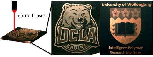
Instead of printing on this specialized coating, here the researchers covered the disk with a film of conducting polyaniline nanofibers, which can then be directly printed on. When light from the infrared laser is absorbed by the nanostructured polyaniline, an unusual photothermic effect occurs, in which the polymer converts most of its absorbed light into heat.
The generated heat then “laser-welds,” or cross-links, the molecular chains and supramolecular fibers together to change the surface morphology of a small area of the polymer. After laser treatment, the welded area of the polymer changes from a tangled nanofibrous mat to a smooth, continuous film as a result of chemical cross-linking. Since polyaniline nanofibers are poor heat conductors, the heat does not spread beyond the laser lines, resulting in a well-defined separation between the welded and non-welded areas. The laser line emitted by the infrared laser in the CD/DVD drive has a diameter of about 0.7-1 µm, allowing for exceptional resolution and precision.
In addition to the high resolution, the laser welding method also provides a high degree of control over the conductivity and optical properties of the welded conducting polymer, which is not possible with previous approaches to polymer patterning. Welded areas demonstrate a significant decrease in film conductivity, which the researchers attribute to the loss of dopants and pi-conjugation during the cross-linking process. They show how printing in grayscale can tune the polymer’s conductivity, with lighter grayscale colors possessing higher conductivity. With the ability to print grayscale colors from white to black, the researchers could tune the polyaniline nanofiber film from semiconductor to insulator, representing a change in conductivity of about 7 orders of magnitude.
Although the idea of using a commercial label-writing system to print organic electronic devices sounds quite simple, Veronica Strong of the University of California, Los Angeles, explained that that doesn’t make it the obvious first choice for a research lab.

“There are several reasons why this technique has not been demonstrated before,” she told PhysOrg.com. “One of these reasons is that, when we began our initial tests, LightScribe had only been around for less than six years. Yet, more importantly, this type of technology is not traditionally found in a laboratory setting nor would it be the first thing to come to mind when testing out ideas. Combining this technology with conducting polymers would have required a research group that was specifically in the market for a new patterning technique and property tuning of conducting polymers. Our group was doing exactly that when the idea was first proposed; in fact, we had just exhausted all the laser technologies that are traditionally used in a laboratory setting. So when a co-worker suggested a DVD player with LightScribe technology, well we just had to try it.”
Among its potential uses, the new technique could also lead to applications through doping. The researchers found that the welded areas no longer respond to reversible doping/dedoping with acids or bases, while the non-welded areas continue to be affected by doping. This property could be especially useful for patterning rechargeable electrodes for batteries or supercapacitors, which benefit from selective doping to enable fast charge/discharge rates.
The researchers also demonstrated that the polymer’s color can be controlled by controlling certain properties, such as the starting oxidation state, the laser intensity, and the extent of cross-linking. Also, different polyaniline derivatives absorb light differently, which leads to additional color variations.
In the future, the researchers plan to further develop this idea by fabricating electronically active devices. They predict that the simple laser welding technique will serve as an important step toward patterning polymer-based organic electronics on a large scale. The technique could be used to pattern a variety of conducting polymer nanofibers in addition to polyaniline, and these polymers can be printed on many different substrates, including paper. Virtually any pattern can be printed, and the same image can be printed repeatedly on the same film in order to increase the contrast. Without the need for photoresists, masks, or post-processing treatment like many other techniques, the new method offers a one-step approach that could potentially have very wide implications.
“Currently, this technique would be especially useful for manufacturing better conducting membranes, microfluidics, and all-organic electronic devices,” Strong said. “The intellectual drive behind this work was to demonstrate that we currently have the tools necessary to make cost-effective, flexible organic and electronically active devices. We hope that we can help drive that out-of-the-box thinking by developing new methods that use our ideas for device manufacturing.”
More information: Veronica Strong, et al. “Direct Sub-Micrometer Patterning of Nanostructured Conducting Polymer Films via a Low-Energy Infrared Laser.” Nano Letters. DOI:10.1021/nl2011593
Copyright 2011 PhysOrg.com.
All rights reserved. This material may not be published, broadcast, rewritten or redistributed in whole or part without the express written permission of PhysOrg.com.


