Bright future for gaN nanowires

The gallium nitride nanowires grown by PML scientists may only be a few tenths of a micrometer in diameter, but they promise a very wide range of applications, from new light-emitting diodes and diode lasers to ultra-small resonators, chemical sensors, and highly sensitive atomic probe tips.
In the two decades since GaN was first employed in a commercially viable LED, ushering in a dazzling future for low-power lighting and high-power transistors, the III-V semiconductor has been produced and investigated numerous ways, in both thin-film and nanowire form.
At PML's Quantum Electronics and Photonics Division in Boulder, CO, much of the recent effort has been devoted to growing and characterizing extremely high-quality GaN nanowires – "some of the best, if not the best, in the world," says Norman Sanford, co-leader of the Semiconductor Metrology for Energy Conversion project.
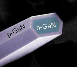
GaN emits light when holes and electrons recombine at a junction created by doping the crystal to create p-type and n-type regions. These layers are formed by a variety of deposition methods, typically on a sapphire or silicon carbide substrate. Conventional methods produce crystals with relatively high defect densities. Unfortunately, defects in the lattice limit light emission, introduce signal noise, and lead to early device failure.
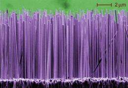
The Boulder team, by contrast, grows virtually defect-free hexagonal GaN nanowires very slowly from a silicon base. Their deposition method is molecular beam epitaxy (MBE) which allows the nanowires to form spontaneously without the use of catalyst particles. Although catalyst particles are widely used for nanowire growth, they leave behind trace impurities that can degrade GaN. It takes two to three days for the structures to reach a length around 10 micrometers (about one-tenth the thickness of a human hair), but the wait pays off because the crystal structure is very nearly perfect.
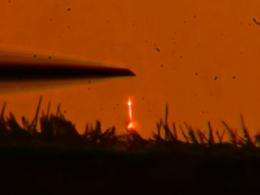
Among other advantages, flawless crystals produce more light. "Now, for the first time, the electroluminescence from a single GaN nanowire LED is sufficiently bright that we can measure its spectrum and track the spectrum with drive current to see evidence of heating," says project co-leader Kris Bertness. "There are no other examples of electroluminescence spectra from a single MBE-grown GaN nanowire in the literature."

GaN and its related alloy system (including semiconductors containing indium and aluminum) form the basis of the rapidly expanding solid state lighting industry. It could move faster, experts believe, if industry could develop an economical method to grow low-defect-density material.
"Conventional GaN-based LEDs grown on cost-effective but non-lattice-matched substrates (such as sapphire) suffer from unavoidable strain and defects which compromise efficiency," Sanford says. "Additionally, light extraction from conventional planar (flat) LED structures is impeded by total internal reflection resulting in wasted photons which are trapped in the device rather than radiating outward as useful light."
GaN nanowire LED technology offers significant improvements since the wires grow essentially free of strain and defects and should thus enable fundamentally more efficient devices. Furthermore, the morphology provided by a "forest" of densely arrayed nanowire LEDs offers improvements in the light-extraction efficiency of these structures compared with their planar counterparts.
Testing and measuring those and other properties, however, poses significant challenges. "P-type GaN is difficult to grow by any common growth method," Bertness says. "And what turns out to be very hard is making good electrical contacts to the nanowire, because it is not flat, and its thickness is larger than most of the metal films used to contact planar films.
"This 3D geometry encourages void formation and trapping of chemical impurities near the contacts, both of which degrade the contact, sometimes to the point of being unusable. This is an area we are actively investigating."
The team is looking at ways to grow nanowires in regular arrays, with careful control of the spacing and dimensions of each individual wire. Recently they found that by creating a grid-like pattern of openings on the order of 200 nanometers wide in a silicon nitride "mask layer" placed over the substrate, they could achieve selective growth of highly regular wires. The ability to produce ordered patterns of uniform GaN devices, Bertness says, "is essential for reliable manufacturing."

GaN is not only a light source. It also has multiple uses in different fields. "Another nice thing about GaN is that it's insensitive to high temperatures," says Robert Hickernell, leader of the Optoelectronic Manufacturing Group, which includes the Semiconductor Metrology project. "That's an advantage for high electrical power applications." The Group is also studying nanowire field effect transistors (FETs) to accurately measure carrier transport properties. "And we've got GaN nanowire FETs that are some of the best research devices in the world."
In addition, GaN nanowires are mechanically robust. Very robust: Four years ago, a PML-University of Colorado collaboration made headlines by producing nanowires with extraordinarily high quality factors that make them potentially excellent oscillators. "In the distant future," Hickernell says, "they might be used in cell phone applications as micro-resonators."
The combination of high mechanical quality factor and tiny mass also makes them capable of detecting masses in the sub-attogram range. PML collaborators at the University of Colorado are confident that they can extrapolate the present experiments to roughly 0.01 attograms, or 10 zeptograms sensitivity. (For comparison, the mass of a virus is on the order of 1 attogram, or 10-18 gram.) No direct measurements have yet been made at that scale.
Earlier this year, Bertness, Sanford and CU collaborators used GaN's native piezoresistance to measure frequency response in nanowires stretched across a 10 micrometer gap. The results showed that the devices had "immediate utility in high-resolution mass and force sensing applications," the researchers wrote in their published report.
The team thinks it is possible to make "a new class of electrically-addressable multifunction scanning-probe tools," Bertness explains. "For example, conventional NSOM relies on a scanning optical tip with an aperture diameter in range of 10 to 100 nanometers which is formed at the tapered end of a passive optical fiber. Those tips are mechanically and chemically fragile and have a very short service life – hours to days. On the other hand, GaN nanowire based NSOM tools can potentially offer electrically-addressable multifunction operation that combines optical emission, optical detection, AFM and RF-AFM functionality."
Finally, GaN nanowires are also well suited for use in chemical, biological, and gas sensing. Ongoing collaborative work between the team and NIST's Material Measurement Laboratory is producing interesting results with GaN nanowires used in tandem with nanoclusters of titanium dioxide to detect aromatic compounds such as benzene and toluene. "Additionally, our project has done some preliminary (published) work with GaN nanowires functionalized for biological molecules," Sanford says. "Various other groups around the world are pursuing similar sensor technology using GaN nanowire backbones."
Provided by National Institute of Standards and Technology


