Microfabrication breakthrough could set piezoelectric material applications in motion

(PhysOrg.com) -- Integrating a complex, single-crystal material with "giant" piezoelectric properties onto silicon, University of Wisconsin-Madison engineers and physicists can fabricate low-voltage, near-nanoscale electromechanical devices that could lead to improvements in high-resolution 3-D imaging, signal processing, communications, energy harvesting, sensing, and actuators for nanopositioning devices, among others.
Led by Chang-Beom Eom, a UW-Madison professor of materials science and engineering and physics, the multi-institutional team published its results in the Nov. 18, issue of the journal Science. (Eom and his students also are co-authors on another paper, "Domain dynamics during ferroelectric switching," published in the same issue.)
Piezoelectric materials use mechanical motion to generate an electrical signal, such as the light that flashes in some children's shoe heels when they stomp their feet. Conversely, piezoelectrics also can use an electrical signal to generate mechanical motion—for example, piezoelectric materials are used to generate high-frequency acoustic waves for ultrasound imaging.
Eom studies the advanced piezoelectric material lead magnesium niobate-lead titanate, or PMN-PT. Such materials exhibit a "giant" piezoelectric response that can deliver much greater mechanical displacement with the same amount of electric field as traditional piezoelectric materials. They also can act as both actuators and sensors. For example, they use electricity to deliver an ultrasound wave that penetrates deeply into the body and returns data capable of displaying a high-quality 3-D image.
Currently, a major limitation of these advanced materials is that to incorporate them into very small-scale devices, researchers start with a bulk material and grind, cut and polish it to the size they desire. It's an imprecise, error-prone process that's intrinsically ill-suited for nanoelectromechanical systems (NEMS) or microelectromechanical systems (MEMS).
Until now, the complexity of PMN-PT has thwarted researchers' efforts to develop simple, reproducable microscale fabrication techniques.
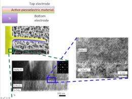
Applying microscale fabrication techniques such as those used in computer electronics, Eom's team has overcome that barrier. He and his colleagues worked from the ground up to integrate PMN-PT seamlessly onto silicon. Because of potential chemical reactions among the components, they layered materials and carefully planned the locations of individual atoms. "You have to lay down the right element first," says Eom.
Onto a silicon "platform," his team adds a very thin layer of strontium titanate, which acts as a template and mimics the structure of silicon. Next comes a layer of strontium ruthenate, an electrode Eom developed some years ago, and finally, the single-crystal piezoelectric material PMN-PT.
The researchers have characterized the material's piezoelectric response, which correlates with theoretical predictions. "The properties of the single crystal we integrated on silicon are as good as the bulk single crystal," says Eom.
His team calls devices fabricated from this giant piezoelectric material "hyper-active MEMS" for their potential to offer researchers a high level of active control. Using the material, his team also developed a process for fabricating piezoelectric MEMS. Applied in signal processing, communications, medical imaging and nanopositioning actuators, hyper-active MEMS devices could reduce power consumption and increase actuator speed and sensor sensitivity. Additionally, through a process called energy harvesting, hyper-active MEMS devices could convert energy from sources such as mechanical vibrations into electricity that powers other small devices—for example, for wireless communication.
The National Science Foundation is funding the research via a four-year, $1.35 million NIRT grant. At UW-Madison, team members include Lynn H. Matthias Professor in Electrical and Computer Engineering Professor Robert Blick and Physics Professor Mark Rzchowski. Other collaborators include people at the National Institute of Standards and Technology, Pennsylvania State University, the University of Michigan, Argonne National Laboratory, the University of California at Berkeley, and Cornell University.
More information: Giant Piezoelectricity on Si for Hyperactive MEMS, Science 18 November 2011: Vol. 334 no. 6058 pp. 958-961 DOI: 10.1126/science.120718 www.sciencemag.org/content/334/6058/958.abstract
Provided by University of Wisconsin-Madison


