A passive alignment method offers an easy solution for fabricating integrated photonic circuits

The rise of computers in past decades was made possible largely thanks to the invention of the integrated circuit, a device that combines all necessary electronic components onto a single chip. In a similar vein, the success of optical computing is largely dependent on the possibility of integrating all essential optical components onto a single chip (photonic circuit). Lim Teck Guan at the A*STAR Institute of Microelectronics and co-workers have now developed an enhanced alignment solution for photonic circuits. “Our approach offers a highly accurate, passive optical alignment solution for these devices,” says Guan.
The fabrication of photonic circuits is no easy task because there is little room for error. In order to get the best performance from these devices operating at the visible or near-infrared spectrum, various elements must be aligned with utmost precision, typically within an error of around one micrometer. Even with the slightest misalignment, a microlens, for example, might not be able to focus light into a photodetector.
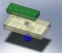
The researchers came up with an alignment method that is remarkably straightforward and easy to implement. It is based on a circular through-hole with two diameters (see image). The design of the larger hole is not critical and it can either partially or entirely accomodate the spherical lens, depending on the application requirement. A second hole in the chip is smaller than the sphere diameter so that if the lens is pressed against the opening the sphere will automatically be aligned in its center. In this way, light from underneath the chip is guided through the lens and the second hole, and on to a photodetector that is placed directly above.
This guided assembly scheme makes it easy to fabricate more complex photonic circuits, once the spherical lenses are integrated with the layer containing the through-holes. Electronic circuits of virtually any complexity can be placed on the chip with high accuracy, so that they align perfectly with the optical beam shone through the lens. The measured efficiencies of the light coupling between the different components on the chip are promising and demonstrate light propagation with few losses.
In the current assembly, a laser is placed on a chip and through a combination of mirrors and microsphere lenses, the light is guided across the chip to a photodetector. However, the researchers have already set their sights on the advantages of further integration. “In future, we might come up with more complex circuits,” suggests Guan. “These devices could lead to applications including high-speed, high-bandwidth integrated photonic circuits, particularly if we can integrate conventional silicon electronics with photonic functionality.”
More information: Guan, L. T. et al. Integrated optical carrier for optical/electrical interconnect. IEEE Transactions on Components, Packaging, and Manufacturing Technology 1, 125–132 (2011). ieeexplore.ieee.org/xpl/freeab … jsp?arnumber=5696784
Provided by Agency for Science, Technology and Research (A*STAR)


