Crystalline materials enable high-speed electronic function in optical fibers

Scientists at the University of Southampton, in collaboration with Penn State University have, for the first time, embedded the high level of performance normally associated with chip-based semiconductors into an optical fibre, creating high-speed optoelectronic function.
The potential applications of such optical fibres include improved telecommunications and other hybrid optical/electronic technologies. This transatlantic team will publish its findings in the journal Nature Photonics this month.
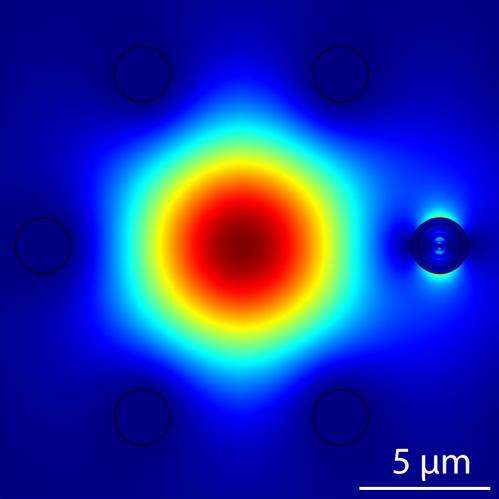
The team has taken a novel approach to the problems traditionally associated with embedding this technology. Rather than merge a flat chip with a round optical fibre, they found a way to build a new kind of optical fibre with its own integrated electronic component, thereby bypassing the need to integrate fibre-optics onto a chip. To do this, they used high-pressure chemistry techniques to deposit semiconducting materials layer by layer directly into tiny holes in optical fibres.
Dr Pier Sazio, Senior Research Fellow in the University of Southampton's Optoelectronics Research Centre (ORC), says: "The big breakthrough here is that we don't need the whole chip as part of the finished product. We have managed to build the junction - the active boundary where all the electronic action takes place - right into the fibre. Moreover, while conventional chip fabrication requires multimillion dollar clean room facilities, our process can be performed with simple equipment that costs much less."

John Badding, Professor of Chemistry at Penn State, explains: "The integration of optical fibres and chips is difficult for many reasons. First, fibres are round and cylindrical, while chips are flat, so simply shaping the connection between the two is a challenge. Another challenge is the alignment of pieces that are so small. An optical fibre is 10 times smaller than the width of a human hair. On top of that, there are light-guiding pathways that are built onto chips that are even smaller than the fibres by as much as 100 times, so imagine just trying to line those two devices up. That feat is a big challenge for today's technology."
Dr Anna Peacock, from the ORC who holds a Royal Academy of Engineering Research Fellowship, adds: "The incorporation of optoelectronic device functionality inside the optical fibre geometry is an important technological advance for future communication networks. In this sense, we can start to imagine a scenario where the data signal never has to leave the fibre for faster, cheaper, more efficient systems."
The research also has many potential non-telecommunications applications. It represents a very different approach to fabricating semiconductor junctions that the team is investigating.
ORC Postdoctoral Researcher, Dr Noel Healy concludes: "This demonstration of complex in-fibre optoelectronic engineering is exciting, as it has the potential to be a key enabling technology in the drive for faster, lower cost, and more energy efficient communication networks."
Provided by University of Southampton


