February 27, 2012 report
NTT researchers develop breakthrough optical memory device

(PhysOrg.com) -- To improve transmission speeds, the Internet has transitioned over the years from one using copper to fiber optic cabling. Unfortunately, this has caused a bottleneck to occur where the light signals meet with electronic circuitry. Researchers have been working for years on a way to make routers, and most particularly, their memory, all optic, to avoid having to convert the signals at all. Now, it appears one such group, NTT, a Japanese telecommunications company, has figured out a way to do it. They describe their work in a paper published in Nature Photonics.
All computer memory is based on a material that is able to have 1s and Os written on to it and held in such a state long enough to be useful. Also necessary is an ability to erase or write over those 1s and Os so that the same memory material can be used over and over.
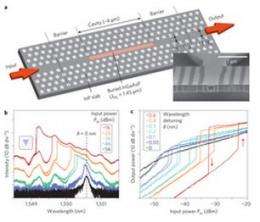
The new memory device created by the NTT team relies on optical cavities that are created in a material that can be made to represent 1s and Os by either transmitting light, or by blocking it.
To make the memory cell, the team buried a very tiny strip of indium gallium arsenide phosphide in a small piece of indium phosphide. The outer portion was then etched with holes small enough to control the flow of laser light of a certain frequency. They left a path running though the middle of the material un-etched to provide a means for light from a laser to move in and out of the cell.
When laser light is shone on the material, it follows the path through the memory cell and the refraction index is changed causing a pulse of light to either pass through on not, representing either a 1 or O state. Another pulse changes it to another state and so on. To help the memory material maintain its state, a second laser provides a constant stream of background light.
The memory cell was able to hold onto the state it created for a microsecond, which quadruples the old record and it also uses far less energy than conventional designs. A memory chip with four of the optical memory cells consumes just 30 millawatts of energy, whereas common use flash drives use five times that amount.
But the real breakthrough here is the development of actual memory cells based on optics that are able to hold onto the data states they create long enough for them to be used by other parts of a hardware device. And while the memory cells are far too large to be of use right now, new designs based on this work might just lead to that elusive Holy Grail, an Internet backbone made entirely of optical components.
More information: Ultralow-power all-optical RAM based on nanocavities, Nature Photonics (2012) doi:10.1038/nphoton.2012.2
Abstract
Optical random-access memory (o-RAM) has been regarded as one of the most difficult challenges in terms of replacing its various functionalities in electronic circuitry with their photonic counterparts. Nevertheless, it constitutes a key device in optical routing and processing. Here, we demonstrate that photonic crystal nanocavities with an ultrasmall buried heterostructure design can solve most of the problems encountered in previous o-RAMs. By taking advantage of the strong confinement of photons and carriers and allowing heat to escape efficiently, we have realized all-optical RAMs with a power consumption of only 30 nW, which is more than 300 times lower than the previous record, and have achieved continuous operation. We have also demonstrated their feasibility in multibit integration. This paves the way for constructing a low-power large-scale o-RAM system that can handle high-bit-rate optical signals.
Journal information: Nature Photonics
© 2011 PhysOrg.com


