NTT develops current-injection photonic-crystal laser
Nippon Telegraph and Telephone Corporation has developed an current-injection photonic-crystal laser with ultralow power consumption that can be applied to off-chip and on-chip optical data transmission for microprocessors.
Microprocessors in servers, routers and other ICT equipment consume a large amount of power. This laser is expected to reduce microprocessor power consumption by approximately 40%.
In addition, the lower power consumption in the ICT equipment will result in reduced heat generation, and can also be expected to reduce the power required for cooling, which currently amounts to about 30% of the power consumed by a data center.
This result will be announced in detail in the February 13 issue of Optics Express, which is published by the Optical Society of America.

The explosive diffusion of broadband services such as FTTH and smartphones will lead to network traffic becoming 200 times greater by 2025. Therefore, the number and capacity of ICT devices such as servers and routers will increase, and it is estimated that the total power consumed by ICT-related devices will have increased fivefold by 2025.
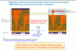
NTT Laboratories have focused on finding a radical solution to the problem of high power consumption and heat generation in ICT equipment by reducing the power consumption of microprocessors (MPU). This is because MPUs consume most of the power in this equipment. In this context, NTT Laboratories have developed optical data transmission technologies for off-chip and on-chip optical interconnection in MPUs.
NTT Laboratories have developed an ultra-compact semiconductor laser consisting of a wavelength-scale active region embedded in a photonic-crystal cavity. This laser achieved the world’s first continuous-wave operation of a current-injection photonic-crystal laser at room temperature (25-30°C). An ultra-low effective operating current of about 10 μA was realized. The output power was 1.8 μW, which is one hundred times the previously reported output power under the pulsed operation of a photonic-crystal laser without an embedded active-region structure. Since the operating characteristics of the current-injection laser are severely degraded at high temperature, continuous-wave operation at room temperature is an indispensable breakthrough technology. These results will make it possible to apply the semiconductor laser to computercom devices.

The energy consumption of a semiconductor laser is lowered by reducing the active volume when the operating carrier density is constant. In addition, high optical confinement is required to achieve laser operation. Conventional nano-cavity lasers cannot control the heat generation in the active region. Therefore, continuous-wave operation at room temperature has not been achieved although many research institutes have attempted to realize a current-injection photonic-crystal laser.
To overcome the problem, NTT Laboratories have developed the LEAP laser. The LEAP laser has achieved continuous-wave operation at room temperature because it incorporates the following features to improve its operating characteristics.

(1) An active region with the smallest reported volume (wavelength(lambda)-scale) is embedded in the photonic-crystal cavity by using nanometer-scale fine selective crystal regrowth and etching technology.
(2) Light and carriers are effectively confined within the ultra-small active region because of the buried heterostructure.
(3) The heat generated in the active region is effectively radiated since the burying InP layer has more than ten times the heat conductivity than the InGaAsP active layer.

The LEAP laser has a pin structure parallel to the substrate, which differs from conventional semiconductor lasers. Therefore, a pin-junction can be formed after crystal growth. The pin structure was formed in the intrinsic InP layer by using the Si ion implantation and Zn diffusion techniques. These techniques will enable the uniform fabrication of large-scale devices as demonstrated with the conventional silicon CMOS process. Therefore, these techniques are suitable for the fabrication of the future large-scale integrated photonic network circuits.
NTT Laboratories is aiming to market ICT equipment in about 2016 in which this laser will be used as an off-chip optical interconnect in an MPU. Next, NTT Laboratories will attempt to fabricate a large-scale photonic network circuit integrated with silicon CMOS by around 2022 to commercialize on-chip data transmission in MPUs. These results will lead to a 40% reduction in the power consumption of such ICT equipment as servers and routers.
Provided by Nippon Telegraph and Telephone Corporation


