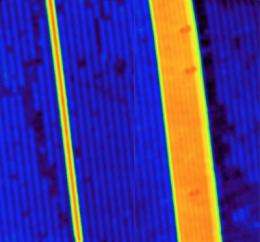
ORNL microscopy explores nanowires' weakest link

Individual atoms can make or break electronic properties in one of the world's smallest known conductors—quantum nanowires. Microscopic analysis at the Department of Energy's Oak Ridge National Laboratory is delivering a rare glimpse into how the atomic structure of the conducting nanowires affects their electronic behavior.
The ORNL team's microscopy confirmed that deliberately introduced defects, which are only the size of a single atom, could turn a conducting nanowire into an insulator by shutting down the path of electrons. Led by ORNL's An-Ping Li, the research team used multiple-probe scanning tunneling microscopy to analyze nanowires made of a material called gadolinium silicide.
"This type of one-dimensional conductor is expected to be a fundamental component in all quantum electronic architectures," said Li, a research scientist at ORNL's Center for Nanophase Materials Science. "One advantage of GdSi2 nanowires is they are compatible with conventional silicon technology and are thus easier to implement in nanoelectronic devices."
The research, published in the American Chemical Society's Nano Letters, is the first correlated study that links electron movement to structural elements such as single point defects or impurities that are intentionally grown in the nanowires.
"When a conductor becomes so small, it will be very sensitive to atomic defects on the nanowire," Li said. "If the conductor or the wire is big, electrons can always find a way to go around. But with such a small nanowire, electrons have no way to escape. When you put only a few defects on this nanowire, you can cut off the conductance and can convert a conductor into an insulator."
Although single nanowires exhibited the metal-to-insulator transition, the ORNL team observed different behavior in bundles of nanowires constructed of two, three or more wires separated by only a few angstroms.
"If you put bundles together, the interwire coupling generally has a stabilizing effect on the structure which in turn leads to better conductance," Li said.
More information: The full paper, "Correlating Electronic Transport to Atomic Structures in Self-Assembled Quantum Wires," is available here: pubs.acs.org/doi/full/10.1021/nl204003s
Provided by Oak Ridge National Laboratory


