February 1, 2012 feature
Engineers build first sub-10-nm carbon nanotube transistor

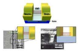
(PhysOrg.com) -- Engineers have built the first carbon nanotube (CNT) transistor with a channel length below 10 nm, a size that is considered a requirement for computing technology in the next decade. Not only can the tiny transistor sufficiently control current, it does so significantly better than predicted by theory. It even outperforms the best competing silicon transistors at this scale, demonstrating a superior current density at a very low operating voltage.
The engineers, from the IBM T.J. Watson Research Center in Yorktown Heights, New York; ETH Zurich in Zurich, Switzerland; and Purdue University in West Lafayette, Indiana, have published their study on the first sub-10-nm CNT transistor in a recent issue of Nano Letters.
Many research groups are working on reducing the size of transistors in order to meet the requirements of future computing technology for smaller, denser integrated circuits. When today’s transistors (silicon metal-oxide-semiconductor field-effect transistors, or Si MOS-FETs) are shrunk, they lose their ability to effectively control electric current, a problem called short-channel effects. For this reason, researchers have been modifying the Si MOS-FET design in an attempt to make the transistor perform better at sub-10-nm gate lengths, but these devices still face performance challenges.
In the new study, the engineers have discarded silicon altogether and turned to single-walled CNTs. Due to their superior electrical properties and ultrathin (1-2-nm diameter) bodies, CNTs have been proposed as a replacement for silicon for several years. Their ultrathin bodies should allow CNTs to maintain gate control of the current in a transistor even at short channel lengths, potentially enabling them to avoid short-channel effects. The IBM team’s sub-10-nm CNT transistor is the first to demonstrate these advantages.
“The greatest significance of this work is in the demonstration that carbon nanotube transistors can not only perform well at sub-10-nm lengths, but that their performance is better than the best-reported Si-based transistors at similar lengths,” IBM researcher Aaron Franklin told PhysOrg.com. “For years it has been known that scaling bulk silicon devices would be extremely challenging, if not impossible, when lengths close in on 10-15 nm….The superb low voltage performance of this scaled carbon nanotube transistor is a sign post showing that there is a demonstrable alternative for extremely scaled transistors.”
Until the engineers built the sub-10-nm CNT transistor, no one knew that they would perform this well. Theories predicted that CNTs with ultrathin channels would experience a loss of gate control as well as a loss of drain current saturation in the output, both of which would degrade performance.
“The reason that theory projected a loss of gate control for nanotube transistors below 15 nm or so (despite their being extremely thin) is related to other unique transport physics for nanotube devices,” Franklin said. “Namely, the carrier effective masses (mass of electrons) are very small for nanotubes compared to other semiconductors, meaning they can tunnel or leak in the device more easily. This is one of the reasons that theories had suggested a loss of gate control, because these 'light' carriers would begin tunneling uncontrollably when the lengths became too small. In the paper, we show that the reason for this discrepancy is largely due to insufficient physics models for transport at the nanotube-metal contacts – previous models mostly ignore what could be happening with electrons getting through the metal-nanotube junction.”
When the engineers fabricated several individual transistors on the same nanotube, the smallest having a channel length of just 9 nm, they observed that the tiniest transistor exhibited superb switching behavior and drain current saturation, defying predictions. When compared to the best-performing sub-10-nm Si transistors of varying designs and diameters, the 9-nm CNT transistor had a diameter-normalized current density of more than four times that of the best silicon transistor. And it exhibited this impressive current density at a low operating voltage (0.5 volts), which is important for reducing power consumption.
The researchers predict that theoretical models can be improved by focusing more on the transport between the metal contacts and CNT. They also think that the high-performing 9-nm CNT transistors demonstrate the potential for using CNT transistors in tomorrow’s computing technology.
“The chief implication is that carbon nanotubes are still worth consideration for a future scaled transistor technology,” Franklin said. “What is often not realized by those outside the field is that carbon nanotube transistors are essentially the only non-silicon devices that have experimentally been shown to have promise in extremely scaled transistors. There are many devices promoted by theory, or demonstrated in larger device structures, but none have been able to show the level of research bench-top performance that nanotubes have. Now, that said, it should be noted that there are challenges ahead before anyone will see an integrated transistor solution from nanotubes. But, to date, nothing related to nanotube transistors has been shown to be fundamentally impossible to solve, from placement of nanotubes in precise locations to the complete separation of metallic and semiconducting nanotubes.”
More information: Aaron D. Franklin, et al. “Sub-10 nm Carbon Nanotube Transistor.” Nano Letters. DOI: 10.1021/nl203701g
Journal information: Nano Letters
Copyright 2012 PhysOrg.com.
All rights reserved. This material may not be published, broadcast, rewritten or redistributed in whole or part without the express written permission of PhysOrg.com.


