July 27, 2007 feature
See-through transistor fabricated for future e-displays

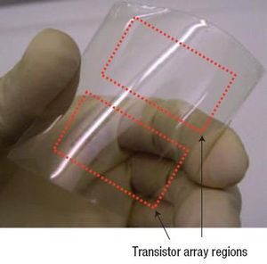
Scientists have recently taken an important step toward the development of “see-through” flexible electronic displays by fabricating fully transparent, high-speed nanowire transistors. This piece of circuitry, the first transistor to demonstrate full transparency, could help turn ideas such as e-paper, displays on sunglasses, and maps on car windshields into a reality.
The collaboration of scientists from Purdue University, Northwestern University, and the University of Southern California, led by David Janes and Tobin Marks, reported their results in a recent issue of Nature Nanotechnology. The group explained that the transparent transistors could be incorporated with active-matrix organic light-emitting diodes (AMOLED), which have already proven to be good transparent pixels.
The transistors’ role in a transparent, flexible display would be to control the flow of current to each pixel. The thin-film transistors (TFTs) utilize wide-bandgap semiconductor nanowires as the active channels, and transparent conducting oxides for the gate, source and drain electrodes.
“While organic TFTs can be made transparent, mobilities in organic TFTs are generally quite low, restricting the speed of operation and requiring relatively large device sizes,” Janes explained to PhysOrg.com. “The reported nanowire TFTs have significantly higher mobilities than other TFT technologies, and therefore offer the potential to operate at much higher speeds. Alternatively, they can be fabricated using much smaller device sizes, which allows higher levels of integration within a given chip area.”
Until now, transistors have not been fully transparent, and so are usually placed around the display. However, transistors that are truly see-through could be located behind or in front of the pixels on a screen, maximizing the screen size and transistor size, which could provide the groundwork for a number of applications.
“Transparent displays are of interest for applications such as heads-up displays on windshields, and informational displays on eyeglasses,” Janes said. “Emerging applications such as ‘e-paper’ require flexible electronics to be integrated within the pixel array. The nanowire transistors demonstrated in this work could operate at much higher speeds, and would allow full-motion video.
“Also, applications such as electronic bar codes, RF ID tags, and smart credit cards would also be advanced by the availability of relatively high performance electronics that could be integrated on a variety of substrates,” he continued. “Flexible circuitry would allow integration on curved and non-rigid surfaces. Transparency would allow integration into multi-layer packaging, in a fashion such that product information could be seen beneath the electronics.”
Not only does the study demonstrate that nanowire electronics can be fully transparent and flexible, but it also shows that such electronics can maintain high performance levels. As Janes mentioned, the high mobility of the transistors means high optical transmission: 90% efficiency for the nanowires alone, and 82% with the glass substrate included.
This high optical transmission, along with the benefits of transparency, would enable the transistors to increase a pixel’s aperture ratio, which is the amount of area within a pixel that transmits light. In AMOLEDs, this improvement would increase efficiency and reduce power consumption—an essential for the many mobile devices researchers hope to create with this circuitry.
Another advantage to the group’s transistors is their simple manufacturing method, which is essential for commercialization. The low-temperature fabrication method will likely allow easy integration onto plastic devices of all sizes.
In the future, one of the biggest challenges researchers will face in improving this technology is controlling the position of the nanowire patterns. For instance, in this sample, the nanowire transistor array regions, which covered just 1 x 0.5 inches, contained 23,000 nanowire patterns. Although there is currently no perfect method for controlling nanowire deposition, the engineers are hopeful that recent advances will continue to improve nanowire orientation.
“Future studies are also expected to include demonstrations of analog and digital circuits based on the nanowire TFTs,” Janes said. “This will require integration of multiple TFTs into an interconnected circuit, as well as development of appropriate interconnect approaches to provide the specific circuit topology.”
Citation: Ju, Sanghyun, Facchetti, Antonio, Xuan, Yi, Liu, Jun, Ishikawa, Fumiaki, Ye, Peide, Zhou, Chongwu, Marks, Tobin J., and Janes, David B. “Fabrication of fully transparent nanowire transistors for transparent and flexible electronics.” Nature Nanotechnology, vol. 2, June 2007, pp. 378-383.
Copyright 2007 PhysOrg.com.
All rights reserved. This material may not be published, broadcast, rewritten or redistributed in whole or part without the express written permission of PhysOrg.com.


