Thin virtual substrates for strained Si

D. Chrastina and his colleagues from the Politecnico di Milano and the ETH Zurich have developed a method to grow thin relaxed SiGe virtual substrates by low-energy plasma-enhanced chemical vapor deposition (LEPECVD). Self-heating of field-effect transistors on these virtual substrates is much reduced while the maximum oscillation and transit frequencies remain very high. LEPECVD is shown to be an excellent deposition technique for next generation integrated circuit technology.
Silicon dominates the electronics market, worth over a hundred billion dollars per year. The next few generations of electronics must therefore be compatible with existing silicon processes. Interest is shifting to virtual substrates of silicon germanium (SiGe) alloys which allow a strained Si layer to be grown. The biaxial tensile strain in the strained Si layer on relaxed SiGe can be tailored by the Ge content. The strain allows the charge carriers to move faster (they have a higher mobility) which in turn means transistors can switch at higher frequencies.
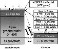
However, the best results for the mobility of the carriers are achieved using a virtual substrate (VS) design which is more than 10 years old: the Ge content of the buffer is graded slowly from zero (pure Si) to around 30% over a few microns.
But SiGe is a terrible thermal conductor so a transistor operating on such a thick VS heats itself up until the advantages of strained Si are more or less lost.
Attention has been focusing on finding a much thinner VS design with acceptable properties.
“We have developed a method to grow thin relaxed SiGe VSs by low-energy plasma enhanced chemical vapour deposition,” says Daniel Chrastina. “Then electrically active layer structures were grown on VSs by molecular-beam epitaxy at DaimlerChrysler AG in Ulm.” (see Fig. 1: Thick and thin LEPECVD virtual substrates side by side, drawn to scale. The factor of ten difference in thickness is evident. The active layer stack for the transistors was grown by molecular-beam epitaxy at DaimlerChrysler AG in Ulm)
Self-heating is much reduced while the maximum oscillation and transit frequencies remain very high. [1, 2]. In fact, in recent “battle of the buffers” [3] transistors on the thin VS reached a maximum oscillation frequency of 121 GHz, beaten only by those on the thick LEPECVD VS. These results show that LEPECVD, with its unrivalled growth rates and flexibility, is a competitive technology for the next generation of integrated electronics.

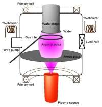
LEPECVD (Fig. 2) uses low-energy dc plasma to speed up the growth of silicon germanium. The plasma conditions cause very efficient cracking of the precursor gas molecules (SiH4 and GeH4) and the low-energy ion bombardment of the surface removes desorbed hydrogen without causing damage to the crystalline structure.
Growth rates of at least 5 nms-1 are available at any substrate temperature and alloy composition, so even a very thick VS can be grown in around 30 minutes. Over the past few years, this technique has been developed at the ETH in Zurich and the L-NESS at the Politecnico di Milano's Como campus. In addition to their own research, they have supplied material to research groups all over Europe and the United States.
The major part of the information for this feature was provided by Dr. Daniel Chrastina. Visit his web-site for more detailed information: www.chrastina.net
References:
[1] T. Hackbarth, H.-J. Herzog, K.-H. Hieber, U. König, M. Bollani, D. Chrastina, and H. von Känel, Appl. Phys. Lett. 83, 5464 (2003).
[2] G. Isella, D. Chrastina, B. Rössner, T. Hackbarth, H.-J. Herzog, U. König, and H. von Känel, Solid State Eletron. 48, 1317 (2004).
[3] M. E. Aguilar, M. Rodriguez, N. Zerounian, F. Aniel, T. Hackbarth, H.-J. Herzog, U. König, S. Mantl, B. Holländer, D. Chrastina, et al., Solid State Eletron. 48, 1443 (2004).


