Copolymers block out new approaches to microelectronics at NIST

In response to the electronics industry’s rallying cry of “smaller and faster,” the next breakthroughs in the electronics size barrier are likely to come from microchips and data storage devices created out of novel materials such as organic molecules and polymers.
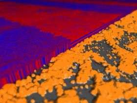
With innovative measurement techniques and new ways to position the molecules, NIST researchers reported at the March Meeting of the American Physical Society how they have improved manipulation of so-called block copolymers—polymers made of a mixture of two or more different molecule building blocks that are tethered at a junction point—which can form arrays of tiny dots that could be used as the basis for electronic components that pack terabytes (1000 gigabytes) of memory in something as small as a pack of gum.
One of the challenges in polymer nanotechnology is how to control their self-assembly—a hard-to-control process for materials which require precision. An important recent NIST accomplishment has been in developing accurate measurements of thin film polymeric nanostructure in 3-D. (Ironically, while determining atomic structure is well-established, measuring the slightly larger internal structure of the polymers—on the order of 10 to 20 nanometers—is much harder.)
Ron Jones, together with colleagues from NIST, the University of Maryland and IBM, has used NIST’s neutron scattering and reflectivity facility to deflect neutrons off block copolymer films from many different angles. By combining the many 2-D neutron scattering pictures into a single composite scattering pattern, this technique provides the first quantitative method for imaging the 3-D internal structure of thin film polymeric nanostructures using neutron scattering—a crucial tool to see if the nanoscale polymer structures are in their required positions.
NIST researchers also have developed new insights on how best to nudge these self-assembling material into those positions. August Bosse will report on computer simulations that model how the polymers assemble when they are placed on templates lined with troughs separated by crests. When a heated zone is swept across the template, the polymer molecules assemble into almost defect free, well-aligned lines faster over the entire template, an important feature for nanotech manufacturing applications.
Sangcheol Kim (working with a team that included researchers from the University of Maryland and IBM) has found that changing the surface chemistry of the template by making some parts hydrophillic and some parts hydrophobic also can elegantly control the dimension of the block-copolymer pattern relative to the chemical template.
And last, with all this emphasis on precise placement, NIST researcher Kevin Yager, has learned that sometimes sloppier is better. By purposely roughening up his templates with a sprinkling of chemically modified nanoparticle silica, he has forced block copolymers into standing perpendicular to the template—a feat that is generally considered tough to manage but important for nanotech applications. Of course, the inner structure of the polymers are not orderly with this technique, but for those applications where only the surface needs to be smooth, this is an ideal, inexpensive way to achieve vertical structures.
Source: National Institute of Standards and Technology


