Low-Temperature Growth and Properties of ZnO Nanowires
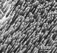
Xuan Wang et al. from Peking University, China report in the last issue of Applied Physics Letters about ZnO nanowires grown through evaporation of zinc powders under a low temperature of 400 C. Being about 10 nm in the diameter these nanowires are long and curved. Typical lengths are tens of micrometers. High-resolution transmission electron microscopy showed that nanowires are mostly crystalline.
Semiconducting nanowires with controlled dimension and morphology will be critical for the fabrication of electronic and optical nanodevices.
ZnO has important application potential owing to its diverse superior properties. For example, ZnO can be used as optical waveguides, transparent electrodes, acousto-optic devices, surface acoustic wave transducers, etc. Its wide band gap of 3.37 eV at room temperature makes ZnO suitable for short-wavelength optoelectronic devices, including light-emitting diodes (LEDs) and laser diodes (LDs). ZnO has a high exciton binding energy of 60 meV, which renders it more applicable for making room-temperature UV laser devices. Small-diameter ZnO nanowires are expected to further lower the lasing threshold because quantum effects result in enhancement of density of states near the band edges and radiative recombination due to carrier confinement.
In the past decade, numerous studies have been made on both production and application of one-dimensional ZnO. Most recently, vapor-phase methods such as thermal evaporation and condensation, carbon thermal-reduction vapor transport, and evaporation of organic zinc precursors have been used. However, most of these processes require synthetic temperature higher than 800 C.
In their study Xuan Wang and colleagues grow ZnO nanowires at 400 C with the assistance of Au nanoparticles. These ZnO nanowires, in the diameter of ~10 nm, are long and curved with lengths of tens of micrometers.
Most of the ZnO nanowires grown are crystalline; however, the kink parts contain dislocations and stacking faults. Researches also observed the movement of dislocations in the kink parts under e-beam irradiation. Besides the structural characterization, they studied photoluminescence and Raman spectra of ZnO nanowires.
This work offers a mild way of producing ZnO nanowires as well as their possible applications.
Read this article in APL (Vol. 84, 24, 4941–4943) for more details.


