A better image for plastic solar cells
A new way to help technologists develop efficient and inexpensive plastic electronic devices, such as plastic solar cells and a new type of transistor was showcased by physicist Andrea Liscio, who is supported by the European Science Foundation, at the EMRS (European Material Research Society) Spring Meeting held in Strasbourg, France at the end of May.
Liscio, a researcher at the Istituto per la Sintesi Organica e la Fotoreattività - Consiglio Nazionale delle Ricerche (CNR) in Bologna, Italy is working in the SUPRAMATES collaborative research project and is using an analytical technique based on a powerful type of microscopy, to analyse materials and map their electrical properties with nanoscopic detail.
Liscio explained how he and his colleagues are using Kelvin Probe Force Microscopy (KPFM), which is an extension of atomic force microscopy, and is 1000 times more powerful than an optical microscope.
He presented details of a systematic study of KPFM measurements of nanostructures. "We studied an extensive range of samples and structures with sizes spanning from several micrometres down to a few nanometres," explained Liscio, "Our results indicated that by operating the KPFM at high frequencies it is possible to visualize different electrical behaviour in nanostructured samples."
A standard AFM has a very sharp probe (just a few atoms across) that scans across a surface the tip bobs up and down following the atomic detail of the surface as forces between the probe and the surface change. The probe's movement is recorded by a highly focused laser linked to a computer. KPFM extends this approach by applying an electric potential to the probe, which allows the electronic properties and composition of the surface to be measured as well as its topography. One property revealed is the work function of the surface, which is linked to a material's catalytic activity, corrosion resistance, and its electronic properties.
"KPFM is a highly versatile tool," explained Liscio, "useful for studying both conducting and semiconducting samples, as well as thin oxide layers, in a non-invasive way."
One group of materials on which the researchers have focused is conjugated nanomaterials. These materials have been widely adopted as the active components of a variety of optoelectronic devices, including organic light-emitting diodes (OLEDs), thin film transistors, solar energy conversion materials.
Optimising such devices depends on being able to fine-tune the movement of electrons at the interface between the electrode and the organic material as well as how they travel through the material. Mapping quantitatively the electronic properties of the surface with a high degree of precision is crucial to this endeavour.
To measure electrostatic interactions, the KPFM probe must be vibrating. As the probe bobs up and down the force required to keep it oscillating at a steady rate changes measurably, which tells the scientists about the nature of the scanned surface. By using different vibration frequencies, it is possible obtain nanoscale measurements on materials.
Liscio and co-workers and others have shown that vibrating the probe above its natural resonant frequency, they could make the device more sensitive.
Liscio explains that within the frame of SUPRAMATES, the collaborative effort is addressing the question of how nanoscale architecture and function are linked. He and his colleagues have a strong interaction with the research groups of Klaus Müllen (MPIP Mainz) and Alan Rowan (Radboud University Nijmegen), which means they can develop new functional nanostructures for testing in organic electronics.
Within these collaborations, the researchers at the CNR Bologna node have used KPFM to investigate organic semiconductors that can undergo self-assembly on a surface to form sophisticated nanoscopic structures and nanofibres of other organic semiconductors, both of which might one day find application in molecular electronics.
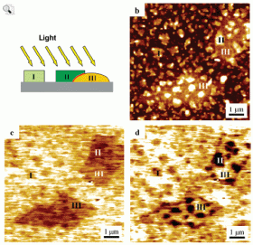
The CNR Bologna team has also applied the technique to studies of organic photovoltaic materials, plastic solar cells in other words, which could significantly cut the costs of renewable solar energy and make it commercially viable. They are testing structurally well-defined plastics known as polyisocyanopeptide polymers as scaffolds on which they can arrange thousands of electron-accepting molecules, among them a group of organic molecules known as the perylene-bis(dicarboximides).
The result is that they can produce hundreds of nanometre-long light-absorbing wires.
They then used KPFM measurements to visualize directly the photovoltaic activity of the nano wires, which offered new insights into how plastic solar cells might be made. Within SUPRAMATES, the performance of devices based on these systems will be explored in the groups of Richard Friend at the University of Cambridge and Franco Cacialli of University College London and the London Center for Nanotechnology.
Source: European Science Foundation


