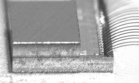
NEC Develops a Three-Dimensional Chip-Stacked Flexible Memory

NEC Corporation announced today the development of chip-stacked flexible memory, which can be used to achieve a new system-on-chip (SoC) architecture. The new SoC's architecture consists of separate logic (excluding embedded memory cores) and memory chips (chip-stacked flexible memory) that are closely stacked by using a three-dimensional packaging technology.
NEC developed both a reconfigurable-memory technology that enables the memory chip to change its configuration flexibly, in addition to a memory-data transmission technology that reduces chip-area and latency caused by memory reconfiguration mechanisms.
The memories of conventional SoCs are categorized into two types; embedded memory, such as embedded SRAM or embedded DRAM, which is integrated with logic circuits in an SoC chip; and the second type, general-purpose memory, such as DRAM or Flash memory, which is placed outside of an SoC chip.
The chip-stacked flexible memory developed by NEC is a third kind of memory that features both fast access in the embedded memory and large memory size in the general-purpose memory. It also enables dynamic memory allocation during LSI operation that is effective in SoC's multiple functional IP-cores (functional blocks), which reduces SoCs' design and fabrication costs.
More details on these technologies:
(1) Reconfigurable-memory technology
Many of the new technology's memory cores are tiled in a memory-specified chip and connected to each other through an interconnect on-chip network. The on-chip network, which is usually used to connect IP cores, is applied to connect memory cores.
Memory configuration becomes programmable by switching network connections, which enables an optimum amount of memory capacity to be allocated flexibly.
(2)Memory-data transmission technology
Time-division multiplex and bit-division multiplex transmission technologies deliver rapid read operations that are comparable to embedded memory.
Using time-division multiplex transmission technology, data from memory cores are time-division multiplexed. Since memory cores share on-chip network switching nodes with neighbor cores, the number of nodes can be reduced. Under bit-division multiplex transmission technology, data are bit-divided and each bit-sliced data goes to a different connection line. Therefore, the number of wires in a line can be reduced by reducing effective bit-width.
By using both transmission technologies, the area for an on-chip network is reduced by about 60% and its latency is also reduced by about 40%. As a result, reconfiguration memory carries out rapid read operations, which are comparable in speed to embedded SRAMs without reconfiguration functions.
In the future, IT/NW appliances will become more important to processing both enormous amounts of data in virtual worlds, as represented by the Internet, but also three-dimensional data or four-dimensional data, which adds a time axis, as represented in the real world by sensor net or image recognition. This data can be capitalized on to provide various functions that suit the needs of companies and individuals alike.
Since an SoC implementing more functions requires larger memory size and more IP cores, it is a challenge to efficiently connect between memory and IP cores.
NEC has already embarked on research to resolve the above issues, and has successfully demonstrated the operation of chip-stacked flexible memory, which delivers large-scale SoCs based on such innovative technologies as on-chip network and 3D packaging.
Although 3D packaging technology is now applicable to multi-stacked general-purpose DRAM, multi-stacked Flash memory and small-packaged imager, there is no suitable 3D packaging technology application for SoC. The development of these technologies is expected to contribute to new applications using 3D packaging technologies that will bring about the realization of a large scale SoC. NEC will continue its development towards a future where large-scale SoCs become a reality.
The results of this research will be presented on February 9th at the International Solid-State Circuit Conference (ISSCC) 2009, held in San Francisco, CA, USA, from February 8th to 12th.
Provided by NEC


