June 1, 2009 feature
Atom Pinhole Camera Acts as a Shrinking Copy Machine

(PhysOrg.com) -- In 1983, Richard Feynman proposed the idea of a machine that could create smaller scale replicas of itself. Today, such a system is still a challenge, but a machine that can produce nanometer-sized copies of micrometer-sized objects could prove to be extremely useful in modern nanotechnologies.
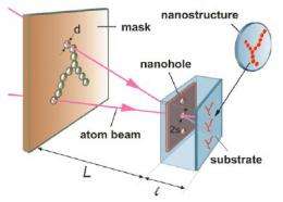
In pursuit of this goal, scientists from the Institute of Spectroscopy, Russian Academy of Sciences have developed a method of nanofabrication using an atom pinhole camera. For the first time, the researchers, along with coauthors from the Moscow Institute of Physics and Technology, have experimentally demonstrated how to use the camera to manufacture an array of identical atomic nanostructures of controlled shapes and sizes. The technique could produce individual nanostructures down to 30 nm, a size reduction of 10,000 times compared with the original object.
“Our present experimental results show the resolution about 30 nm, but our calculations (the theoretical prediction) tell us that the resolution can be down to about 6 nm,” Victor Balykin of the Russian Academy of Sciences told PhysOrg.com.
As the scientists explain, the atom pinhole camera they designed is based on the idea of an optical pinhole camera, which is often used in optics when creation of a focusing lens is difficult. Instead of light traveling through a lens, light travels through a pinhole on a mask, and creates an inverted image on a substrate on the other side. Optical pinhole cameras can produce high-quality images with high resolution that depends on the diameter of the pinhole.
In an atom pinhole camera, atoms act like photons in an optical pinhole camera, and so the main principles are the same in both versions. In their experimental setup, the scientists used ion beam milling to poke a pinhole in a mask. After the atoms passed through the pinhole, they created an atomic nanostructure on a silicon substrate. As the atom pinhole camera provides a way to replicate micro-sized objects as nano-sized ones, the camera is an example of Feynman’s scalable manufacturing system.
The scientists also created another mask with a large array of pinholes. In this “atom multiple pinhole camera,” each pinhole could generate its own image, which does not intersect with neighboring images. As the scientists noted, a camera with up to 10 million pinholes could open up opportunities for simultaneous generation of large numbers of identical (or diverse) nanostructures.
Using an atom pinhole camera to fabricate nanostructures offers several advantages compared to other nanofabrication techniques, which include optical photolithography (in which a photosensitive material is molded by light), nanolithography (in which focused particle beams mold objects), and atom optics methods that use lenses, which are limited by diffraction.
“Presently there are many different methods to build the nanostructures on a surface but usually they are very complicated, limited in choice of materials, and costly,” Balykin said. “Our machine can be built in any lab (with reasonable efforts and by a PhD student) and it will produce a necessary nanostructure.”
The atom pinhole camera is a novel type of lens-less atom optics technique, which uses diffraction to its advantage. While it might seem that resolution in atom pinhole camera would be limited to the diameter of the pinhole, the researchers show in an upcoming study that the image spot diameter can be three times smaller than the pinhole diameter, which is due to diffraction effects.
The new method can be used with a variety of materials for nanostructures (e.g. atoms, molecules, and clusters) and a variety of substrates, which could make it useful for diverse applications such as electronics and biological uses. The scientists predict that the method could have applications in metamaterials, plasmonics, spintronics, MEMS/NEMS, and more.
More information: P.N. Melentiev, A.V. Aablotskiy, D.A. Lapshin, E.P. Sheshin, A.S. Baturin, and V.I. Balykin. “Nanolithography based on an atom pinhole camera.” Nanotechnology 20 (2009) 235301 (7pp).
Copyright 2009 PhysOrg.com.
All rights reserved. This material may not be published, broadcast, rewritten or redistributed in whole or part without the express written permission of PhysOrg.com.


