Graphene -- the copy beats the original

July 17, 2009 Graphene -- the copy beats the original

Enlarge

(PhysOrg.com) -- The first artificial graphene has been created at the NEST laboratory of the Italian Institute for the Physics of Matter (INFM-CNR) in Pisa. It is sculpted on the surface of a gallium-arsenide semiconductor, to which it grants the extraordinary properties of the original graphene. Published as a Rapid Communication on Phys.Rev.B, the research has been highlighted by the American Physical Society.

They envisioned it at the NEST laboratory in Pisa (a joint INFM-CNR and Scuola Normale Superiore di Pisa lab), and then they “sculpted” it like a work of art on the surface of a semiconductor. They named it “artificial ”, the very first ever created, ready to raise the interests of both industry and research. This amazing “copy” promises to render available the incredible electronic qualities of graphene, and thus, it offers a way to overcome the closing physical limits that plague silicon. An exceptional result of Marco Gibertini, Achintya Singha, Marco Polini and Vittorio Pellegrini of INFM-CNR and Scuola Normale Superiore di Pisa, with the cooperation of Giovanni Vignale (University of Missouri), Aron Pinczuk (Columbia University) Loren Pfeiffer and Ken West (Alcatel-Lucent’s Bell Labs).

Natural graphene is an interesting but elusive material, observed for the first time in 2004. It has a very peculiar structure, being composed of a single layer of (only one atom thick) arranged in a grid which resambles common chicken wire. This structure grants graphene its exciting : over this two-dimensional carbon nanoworld, electrons move almost freely at very high speeds, acting like massless particles. For the electronic industry, this means more efficient devices that will be able to be built a lot smaller than what silicon allows. Such an innovation, however, is yet far away to come, because production of graphene with sizes and reproducibility needed by the is not possible yet.

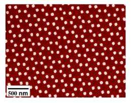
But, if currently-out-of-our-reach graphene offers so many desirable qualities, why not try to “trick” nature and “steal” its qualities creating a copy? An entriguing route, based on the idea that replicating graphene’s structure on a different material might endow it with graphene’s extraordinary properties. And this is exactly what that scientists at NEST tried with the help of gallium-arsenide semiconductors, objects widespread in the production of transistors and lasers. They carved a semiconductor with the help of an ion beam, creating a nanopattern on its surface that replicates the exact graphen’s structure. And the idea proved to be a complete success: modified in this way, the nanosculptured semiconductor exhibits the properties of the famous material it imitates, thus becoming the very first artificial graphene. With an added advantage: the overall procedure does not rely on exotic equipments, but on tools and instruments that the nanofabrication industry already possesses and masters, meaning that the artificial graphene can already enable the development of high-mobility transistors and lasers.

“We are extremely happy” commented Vittorio Pellegrini and Marco Polini “to have been first in creating artificial graphene. This line of research has a great strategic importance, and for this reason very intense competition had sparkled between many research groups around the world. Being the first to create this material means in fact gaining a significant advantage in exploiting its extraordinary characteristics. And we believe that this ‘artificial copy’, already part of a semiconductor, may finally make graphene’s properties available to be implemented in industrial projects and products.”

More information: Phys. Rev. B 79, 241406(R) (2009); doi:10.1103/PhysRevB.79.241406

Provided by National Institute for the Physics of the Matter


print this article email this article download pdf blog this article bookmark this article     Stumble it Digg this share on Facebook retweet share on Reddit add to delicious
Rate this story - 4.9 /5 (25 votes)

Rank Filter

Move the slider to adjust rank threshold, so that you can hide some of the comments.


Display comments: newest first

  • zevkirsh - Jul 17, 2009
    • Rank: 5 / 5 (1)
    form over function. its not the material, its the shape. meta materials here we come. now why not try doing this with silicon?
  • jimbo92107 - Jul 17, 2009
    • Rank: 5 / 5 (2)
    Not the best explanation of the phenomenon. What are those white dots, holes or bumps? What's the chemical difference between the white dots and the red background? What's the size of the pattern? Little details like that are the meat of the issue.
  • PinkElephant - Jul 17, 2009
    • Rank: not rated yet
    A puzzling phenomenon. Why would restricting degrees of freedom, increase mobility? This kind of patterning effectively reduces the cross-section of semiconductor through which electrons can move -- and yet it makes the movement easier. What's the physical basis for this effect?
  • tola1 - Jul 17, 2009
    • Rank: not rated yet
    So, we have somewhat affordable strong material carved on another material, but we dont have light and strong material by itself? No affordable space elevator cable material yet?
  • NeilFarbstein - Jul 17, 2009
    • Rank: 1 / 5 (1)
    Don't steal graphene patterns you will be caught and prosecuted. Besides artificial graphite has already been invented. It forms on top of nickel under the right conditions.R.E. Smalley's group discovered that when they were researching catalysts of carbon nantubes.
  • mattytheory - Jul 17, 2009
    • Rank: 5 / 5 (1)
    Not the best explanation of the phenomenon. What are those white dots, holes or bumps? What's the chemical difference between the white dots and the red background? What's the size of the pattern? Little details like that are the meat of the issue.

    the authors state that the atoms are arranged in a pattern that resembles chicken wire and that the sheet is one atom thick. chicken wire is hexagonal, if you have ever seen it, and if you look at the picture, you can clearly make out the hexagonal pattern of white dots on a red background. i would say that the white dots are individual carbon atoms arranged artificially to create a sheet of graphene. the scale is 500nm, which looks to be about 1.5 times the size of one of the hexagonal arrangements. as to chemical difference, i will wait for someone else to give their thoughts.


    form over function. its not the material, its the shape. meta materials here we come. now why not try doing this with silicon?


    maybe form determines function??
  • daveib6 - Jul 18, 2009
    • Rank: 5 / 5 (1)

    i would say that the white dots are individual carbon atoms arranged artificially to create a sheet of graphene.

    I believe you have all misunderstood the meaning of this article. They have created 'Artificial Graphene'. That does not imply that it is made out of carbon, but that it's form is the same as graphene. The point is that it is on a nano-scale LIKE graphene in that it is a one-dimensional material in the same hexagonal pattern. This meta-material is still made out of GaAs, but its' function is similar to graphene because its' form is identicle to graphene. If they can do this with GaAs, it may be possible to do it also with Silicon (since in principle all 3 share the chemical properties which allow all 3 to be crystalized in the diamond structure), although my guess is that it will be much harder. Harder yet would be Germainium-Silicon which has become the main stay of the 45mn node.
  • mattytheory - Jul 18, 2009
    • Rank: 5 / 5 (1)
    @daveib6: you are correct i concede. i found the paper online... i dont have the $25 to buy it but the abstract is really good and, in some ways, explains what the researchers were doing better than this article. anyways, here is the link:
    http://physics.ap...9.241406

    cheers
  • NeilFarbstein - Aug 04, 2009
    • Rank: 1 / 5 (1)
    A puzzling phenomenon. Why would restricting degrees of freedom, increase mobility? This kind of patterning effectively reduces the cross-section of semiconductor through which electrons can move -- and yet it makes the movement easier. What's the physical basis for this effect?

    I cars lined up on roads will travel soothly instead of all of them driving and hitting each other at random.

July 17, 2009 all stories

Comments: 9

4.9 /5 (25 votes)
  • Stumble this up

  • Digg this

  • share this

  • hide
  • Related Stories

  • Light-speed nanotech: Controlling the nature of graphene
    created Jan 21, 2009 | popularity not rated yet | comments 0
  • Could Graphene Replace Semiconductors?
    created Sep 08, 2008 | popularity not rated yet | comments 0
  • Graphene makes movement easy for electrons
    created Jan 08, 2008 | popularity not rated yet | comments 0
  • Scientists discover ground-breaking material: Graphane
    created Jan 30, 2009 | popularity not rated yet | comments 0
  • A Smarter Way to Grow Graphene
    created May 14, 2008 | popularity not rated yet | comments 0


  • hide
  • Relevant PhysicsForums posts

  • Physics of Golf
    created 1hour ago
  • Rocket Experiment Help
    created 11 hours ago
  • Coulomb's Law
    created 16 hours ago
  • Laser spots
    created 20 hours ago
  • Do you know elementary physics?
    created 22 hours ago
  • Bicycles and their mad skillz
    created 23 hours ago
  • More from Physics Forums - General Physics

Other News

Nanoparticles used in common household items caused genetic damage in mice

Nanotechnology / Bio & Medicine

created Nov 16, 2009 | popularity 4.8 / 5 (24) | comments 11

Titanium dioxide (TiO2) nanoparticles, found in everything from cosmetics to sunscreen to paint to vitamins, caused systemic genetic damage in mice, according to a comprehensive study conducted by researchers at UCLA's Jonsson ...


Nanotube defects equal better energy and storage systems

Nanotube defects equal better energy and storage systems

Nanotechnology / Nanomaterials

created Nov 19, 2009 | popularity 4.4 / 5 (10) | comments 2

(PhysOrg.com) -- Most people would like to be able to charge their cell phones and other personal electronics quickly and not too often. A recent discovery made by UC San Diego engineers could lead to carbon ...


Using superconducting probes to get a picture of what it's like inside CNTs

Nanotechnology / Nanophysics

created Nov 20, 2009 | popularity 4.9 / 5 (8) | comments 0

(PhysOrg.com) -- "Carbon nanotubes are exciting for fundamental physics, and for potential technological applications," Nadya Mason tells PhysOrg.com. "However, we are generally limited in the way that we can study them. ...


New study confirms exotic electric properties of graphene

New study confirms exotic electric properties of graphene

Nanotechnology / Nanomaterials

created Nov 17, 2009 | popularity 4.8 / 5 (23) | comments 1

(PhysOrg.com) -- First, it was the soccer-ball-shaped molecules dubbed buckyballs. Then it was the cylindrically shaped nanotubes. Now, the hottest new material in physics and nanotechnology is graphene: ...


Small optical force can budge nanoscale objects

Small optical force can budge nanoscale objects

Nanotechnology / Nanophysics

created Nov 17, 2009 | popularity 4.8 / 5 (12) | comments 0

(PhysOrg.com) -- Engineering researchers have used a very tiny beam of light with as little as 1 milliwatt of power to move a silicon structure up to 12 nanometers.