Researchers simplify fabrication of nano storage, chip-design tools
Advances by the Rice University lab of James Tour have brought graphite's potential as a mass data storage medium a step closer to reality and created the potential for reprogrammable gate arrays that could bring about a revolution in integrated circuit logic design.
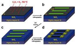
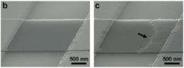
In a paper published in the online journal ACS Nano, Tour and postdoctoral associate Alexander Sinitskii show how they've used industry-standard lithographic techniques to deposit 10-nanometer stripes of amorphous graphite, the carbon-based, semiconducting material commonly found in pencils, onto silicon. This facilitates the creation of potentially very dense, very stable nonvolatile memory for all kinds of digital devices.
With backing from a major manufacturer of memory chips, Tour and his team have pushed the technology forward in several ways since a paper that appeared last November first described two-terminal graphitic memory. While noting advances in other molecular computing techniques that involve nanotubes or quantum dots, he said none of those have yet proved practical in terms of fabrication.
Not so with this simple-to-deposit graphite. "We're using chemical vapor deposition and lithography -- techniques the industry understands," said Tour, Rice's Chao Professor of Chemistry and a professor of mechanical engineering and materials science and of computer science. "That makes this a good alternative to our previous carbon-coated nanocable devices, which perform well but are very difficult to manufacture."
Graphite makes a good, reliable memory "bit" for reasons that aren't yet fully understood. The lab found that running a current through a 10-atom-thick layer of graphite creates a complete break in the circuit -- literally, a gap in the strip a couple of nanometers wide. Another jolt repairs the break. The process appears to be indefinitely repeatable, which provides addressable ones and zeroes, just like today's flash memory devices but at a much denser scale.
Graphite's other advantages were detailed in Tour's earlier work: the ability to operate with as little as three volts, an astoundingly high on/off ratio (the amount of juice a circuit holds when it's on, as opposed to off) and the need for only two terminals instead of three, which eliminates a lot of circuitry. It's also impervious to a wide temperature range and radiation; this makes it suitable for deployment in space and for military uses where exposure to temperature extremes and radiation is a concern.
Tour's graphite-forming technique is well-suited for other applications in the semiconductor industry. One result of the previous paper is a partnership between the Tour group and NuPGA (for "new programmable gate arrays"), a California company formed around the research to create a new breed of reprogrammable gate arrays that could make the design of all kinds of computer chips easier and cheaper.
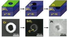
The Tour lab and NuPGA, led by industry veteran Zvi Or-Bach (founder of eASIC and Chip Express), have applied for a patent based on vertical arrays of graphite embedded in "vias," the holes in integrated circuits connecting the different layers of circuitry. When current is applied to a graphite-filled via, the graphite alternately splits and repairs itself (a process also described in the latest paper), just like it does in strip form. Essentially, it becomes an "antifuse," the basic element of one type of field programmable gate array (FPGA), best described as a blank computer chip that uses software to rewire the hardware.
Currently, antifuse FPGAs can be programmed once. But this graphite approach could allow for the creation of FPGAs that can be reprogrammed at will. Or-Bach said graphite-based FPGAs would start out as blanks, with the graphite elements split. Programmers could "heal" the antifuses at will by applying a voltage, and split them with an even higher voltage.
Such a device would be mighty handy to computer-chip designers, who now spend many millions to create the photolithography mask sets used in chip fabrication. If the design fails, it's back to square one.
"As a result of that, people are only hesitantly investing in new chip designs," said Tour. "They stick with the old chip designs and make modifications. FPGAs are chips that have no specific ability, but you use software to program them by interconnecting the circuitry in different ways." That way, he said, fabricators don't need expensive mask sets to try new designs.
"The No. 1 problem in the industry, and one that gives an opportunity for a company like ours, is that the cost of masks keeps moving up as people push semiconductors into future generators," said Or-Bach. "Over the last 10 years, the cost of a mask set has multiplied almost 10 times.
"If we can really make something that will be an order of magnitude better, the markets will be happy to make use of it. That's our challenge, and I believe the technology makes it possible for us to do that."
More information: The ACS Nano paper appears here: pubs.acs.org/doi/pdf/10.1021/nn9006225
Source: Rice University (news : web)


