Fujitsu Develops Technology for Low-Temperature Full-Service Direct Formation of Graphene Transistors on Large-Scale Sub

Fujitsu Laboratories today announced, as a world first, the development of a novel technology for forming graphene transistors directly on the entire surface of large-scale insulating substrates at low temperatures while employing chemical-vapor deposition (CVD) techniques which are in widespread use in semiconductor manufacturing.
Compared to the temperatures of 800-1000°C at which graphene is formed with conventional methods, Fujitsu has succeeded in significantly lowering the graphene fabrication-temperature to 650°C, thus allowing for graphene transistors to be formed directly on a variety of insulator substrates, including substrates that are sensitive to the higher temperatures. Graphene is a nano-scale carbon material (nano-carbon) with the potential to be the material used in next-generation low-voltage, low-power transistors, as graphene features high-electron and hole mobility characteristics.
Details of this technology will be presented at the Materials Research Society 2009 (MRS 2009) Fall Meeting, to be held from November 30 to December 4 in Boston.
Currently, silicon is the material used for transistor channels - the conduits that pass electricity - in LSIs, and through miniaturization of devices, higher speeds and lower power consumption have been realized. However, in recent years, miniaturization technology has been approaching its limits, and achieving further higher performance is becoming increasingly more difficult. This issue has led to a wave of active development of next-generation transistors using materials such as germanium, gallium arsenide, or graphene as channel materials.
Graphene is essentially a single layer of the multi-layered graphite that is used, for example, as pencil lead. The individual carbon atoms in graphene are linked into a hexagonal lattice that is laid out in a flat sheet (Figure 1). Single sheets of graphene were first separated successfully in 2004, and were found to feature excellent electrical characteristics. Experiments showed that graphene has extremely high electron mobility compared to silicon that is typically used in semiconductors, and it is anticipated that graphene could be used to produce fast, low-voltage transistors.
 substrate (wafer) with oxide film")
Prototype transistors using graphene have been produced since several years ago. Laying the graphene on the substrate involved one of the following procedures:
1. Peel-off/transfer method
A method in which a layer is peeled off from a graphite crystal using tape, and transferred to the substrate.
2. CVD/transfer method
A method in which graphene is formed on a film of metallic catalyst at temperatures of approximately 800-1000°C, and then transferred to a different substrate.
3. Silicon-carbide (SiC) surface decomposition method
A method in which a substrate of SiC, a semiconductor, is heat-treated at 1200-1500°C to form graphene on the SiC surface.
The CVD/transfer method using a metallic catalyst has the advantage that graphene can be formed on any kind of substrate, but because it is impossible to form transistors on conductive metal, the graphene that had been formed on one substrate would be transferred to an insulating substrate to make the transistors. The CVD/transferring method is prone to forming wrinkles in the thin-film graphene, and is not readily amenable to use with the 300-mm wafer size that is common today. Practical implementation of the CVD/transferring method would require the ability to produce transistors that are consistent regardless of substrate size.
An additional issue is that as graphene transistors are usually formed at temperatures of 800°C or higher, there was a limit to the types of substrates that graphene could be used with.

Overview of Fujitsu's Newly-Developed Technology
As a world first, Fujitsu Laboratories developed novel technology that allows for graphene to be formed on insulating film substrate via CVD at the low fabrication-temperature of 650°C, enabling graphene-based transistors to be directly formed on the entire surface of substrates. Although the test substrate employed was a 75-mm silicon substrate (wafer) with oxide film, the new technique is applicable to larger 300-mm wafers as well (Figure 2). Key details of the new technology are as follows:
1. Low-temperature synthesis of multi-layer graphene featuring thickness controlled via CVD, on entire surface of substrate
Fujitsu Laboratories developed technology in which an iron film catalyst is deposited on a silicon substrate with oxide film, and on top of that, a layer of graphene is formed to a controlled thickness via CVD with acetylene as the feedstock. As illustrated in Figure 3, this technique can be used to form graphene in varied thicknesses anywhere from 1 nm - for few-layer graphene - to 50 nm, for multi-layer graphene. Furthermore, Fujitsu Laboratories' proprietary CVD technology enables a synthesis temperature of 650°C to be achieved, as compared with the typical 800-1000°C, thereby indicating that graphene could be formed on various substrate surfaces other than silicon - such as glass, which is vulnerable to heat.
2. Process for forming transfer-free graphene transistors
Fujitsu Laboratories also developed a process for forming transistors that use graphene as the channel material (Figure 4), as outlined below. This process is independent of wafer size, so it can be applied to large-scale substrates.
1. First, an iron catalyst is formed into the desired channel shape, using a conventional photolithographic process.
2. Graphene is then formed on the iron layer via CVD.
3. Source and drain electrodes of titanium-gold film are formed at both ends of the graphene, thereby "fixing" the graphene.
4. Next, just the iron catalyst is removed using acid, leaving the graphene suspended between the source and drain electrodes, with the graphene "bridged" between the electrodes.
5. Using atomic-layer deposition (ALD), a method for forming thin films, a layer of hafnium dioxide (HfO2) is grown on top of the graphene to stabilize the graphene.
6. Finally, a gate electrode is formed on top of the graphene and through the HfO2, resulting in the formation of a graphene transistor.

In order for the performance of graphene transistors to be improved, it is essential that graphene can be formed so that it is suspended in air - as aforementioned in "4" above - so that both sides of the graphene can be cleaned. The ALD method employed by Fujitsu Laboratories allows for the formation of insulator film so that it covers the graphene suspended in air (Figure 5).
This new technology from Fujitsu Laboratories enables successful formation of graphene transistors across the entire surface of a large substrate. Figure 6 illustrates an example of the relationship (dependency) between drain current and gate voltage for a top-gate graphene transistor. The figure clearly shows the ambipolar characteristics that are particular to graphene.
As graphene at the thickness of a few nanometers is transparent and passes light well, it is a candidate for use as the channel and electrode material in thin-film transistors used in video displays. With Fujitsu Laboratories' new technology the graphene-forming temperature is approximately 650°C, and is not far from the temperature of approximately 550°C at which graphene could be formed directly on conventional glass. Thus, it is feasible that in the near future it may be possible to form graphene transistors directly on large glass substrates.
-
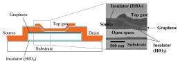
Figure 5: Schematic diagram of a suspended graphene transistor and its cross-sectional Transmission Electron Microscope (TEM) image -
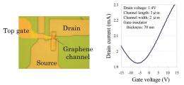
Figure 6: Optical microscope image of a top-gate transistor and its cross-sectional Transmission Electron Microscope (TEM) image
Provided by Fujitsu Laboratories


