Next generation devices get boost from graphene research

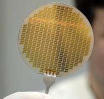
(PhysOrg.com) -- Researchers in the Electro-Optics Center (EOC) Materials Division at Penn State have produced 100 mm diameter graphene wafers, a key milestone in the development of graphene for next generation high-power, high-frequency electronic devices.
Graphene is the two-dimensional form of graphite and consists of tightly bound carbon atoms in a hexagonal arrangement resembling chicken wire. Thanks to the ability of an electron to move at 1/300th the speed of light through graphene (significantly faster than silicon), graphene is a candidate material for many high-speed computing applications in the multibillion-dollar semiconductor device industry.
The Penn State EOC is a leading center for the synthesis of graphene materials and graphene-based devices. Using a process called silicon sublimation, EOC researchers David Snyder and Randy Cavalero thermally processed silicon carbide wafers in a high temperature furnace until the silicon migrated away from the surface, leaving behind a layer of carbon that formed into a one- to two-atom-thick film of graphene on the wafer surface. The EOC wafers were 100mm in diameter, the largest diameter commercially available for silicon carbide wafers, and exceeded the previous demonstration of 50mm.
According to EOC materials scientist Joshua Robinson, Penn State is currently fabricating field effect transistors on the 100 mm graphene wafers and will begin transistor performance testing in early 2010. A further goal is to improve the speed of electrons in graphene made from silicon carbide wafers to closer to the theoretical speed, approximately 100 times faster than silicon. That will require improvements in the material quality, says Robinson, but the technology is new and there is plenty of room for improvements in processing.
In addition to silicon sublimation, EOC researchers Joshua Robinson, Mark Fanton, Brian Weiland, Kathleen Trumbull and Michael LaBella are developing the synthesis and device fabrication of graphene on silicon as a means to achieve wafer diameters exceeding 200mm, a necessity for integrating graphene into the existing semiconductor industry. With the support of the Naval Surface Warfare Center in Crane, Ind., EOC researchers are initially focusing on graphene materials to improve the transistor performance in various radio frequency (RF) applications.
With its remarkable physical, chemical and structural properties, graphene is being studied worldwide for electronics, displays, solar cells, sensors, and hydrogen storage. Graphene has the potential to enable terahertz computing, at processor speeds 100 to 1,000 times faster than silicon. For a material that was first isolated only five years ago, graphene is getting off to a fast start.
Provided by Pennsylvania State University


