February 21, 2010 weblog
3-D Chip Design Challenges

(PhysOrg.com) -- With the increase functionality of electronic gadgets, the need to pack more transistors into a single package is becoming a needed necessity. There’s a big demand, in the consumer market, for smaller packages and in order to meet this demand, 3-D chip technology must be perfected.
By using 3-D design technology, it’s possible to pack more transistors on a single chip as traditional 2-D scaling slows down. There is however design challenges that need to be overcome before 3-D chips become a reality.
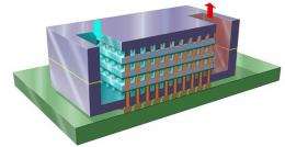
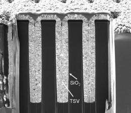
At the IEEE International Solid-State Circuit Conference, this February, Imec engineers presented some key design challenges of 3-D chips made by stacking layers of silicon dies using vertical copper interconnects called TSVs (through-silicon vias). Imec is one of Europe’s largest independent research centers in nano-electronics and nano-technology. They employ over 1,650 people from all over the world to work at IMEC’s campus.
By using TSVs larger bandwidths between memory and logic can exist. Traditional wire interconnects limits bandwidth and consumes more space. This limits the processing speed and consumes power while increasing latency; this in turn creates bandwidth bottlenecking. Because TSVs are typically placed 200 micrometers apart, bandwidth bottlenecking can be greatly reduce.
Heat is another problem for TSVs because the thermal characteristics are three times more critical in 3-D structures as compared to 2-D ones. The poorly conductive adhesives, that hold the thin wafers together, don’t evenly spread the heat through the chip thereby causing hotspots. This can cause reliability issues in the chip and data corruption.

Mechanical stress is also a concerning factor because the copper TSVs contract faster when they are cooling than their silicon counterpart. Too much stress can hinder transistor performance.
The placement of TSVs to transistors on the chip can change chip parameters such as threshold voltage and drive current. Designers will need to compensate for this by creating blank areas or gaps on the chip that would have no devices.
3-D chip designers will have to consider all these factors and carefully balance the cost of the modified architecture that TSVs require in order to have any significant benefits.
More information: www.prism.gatech.edu/~rgoel3/GTCAD/ICCAD.pdf
© 2010 PhysOrg.com


