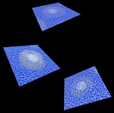
Revolutionary New Solution for Semiconductor, Nano Materials

(PhysOrg.com) -- University of Maryland researchers have created a completely new way to produce high quality semiconductor materials critical for advanced microelectronics and nanotechnology. Published in the March 26 issue of Science, their research is a fundamental step forward in nanomaterials science that could lead to significant advances in computer chips, photovoltaic cells, biomarkers and other applications, according to the authors and other experts.
"This is a major, major advance that shows it is possible to do something that was impossible to do before," said Massachusetts Institute of Technology Associate Professor Francesco Stellacci, whose own work focuses on discovery of new properties in nanoscale materials and the development of new nanofabrication schemes. "This research actually shows that it's possible at the nanoscale for two materials to happily coexist at their interface, two materials that would not coexist otherwise," explained Stellacci, who was not involved in the study.
Led by Min Ouyang, an assistant professor in the department of physics and the Maryland NanoCenter, the University of Maryland team has created a process that uses chemical thermodynamics to produce, in solution, a broad range of different combination materials, each with a shell of structurally perfect mono-crystal semiconductor around a metal core.
Ouyang and fellow researchers Jiatao Zhang, Yun Tang and Kwan Lee, say their method offers a host of benefits over the existing process, known as epitaxy, used to create single crystal semiconductors and related devices. The biggest advantage of their non-epitaxial process may be that it avoids two key constraints of epitaxy -- a limit on deposition semiconductor layer thickness and a rigid requirement for "lattice matching."
The constraints of the epitaxial method restrict the materials that can be formed with it. For example, authors Ouyang, Zhang, Tang and Lee note that attempts to use epitaxy to achieve the kind of hybrid core-shell nanostructures they demonstrate in their article have been unsuccessful.
"Our process should allow creation of materials that yield highly integrated multi-functional microelectronic components; better, more efficient materials for photovoltaic cells; and new biomarkers," said Ouyang, who noted his team is in the process of applying for a patent. "We envision for example that we can use this method to create new types of photovoltaic cells that are ten times more efficient in converting sunlight to electricity than current cells.
"Our method doesn't require a clean room facility and the materials don't have to be formed in a vacuum the ways those made by conventional epitaxy do," Ouyang said. "Thus it also would be much simpler and cheaper for companies to mass produce materials with our process."
Epitaxy is one of the cornerstones of contemporary semiconductor industry and nanotechnology. It has been considered the most affordable method of high quality crystal growth for many semiconductor materials including silicon-germanium, gallium nitride, gallium arsenide, indium phosphide and graphene.

A Quantum Leap
The new method also can be used to design and fabricate artificial quantum structures that help scientists understand and manipulate the basic physics of quantum information processing at the nanoscale, said Ouyang, noting that he and his team have a separate paper on the quantum science applications of this method that they expect to be published in the near future.
This work was supported by the Office of Naval Research, the National Science Foundation (NSF) and the Beckman Foundation. Facility support was from Maryland Nanocenter and its Nanoscale Imaging, Spectroscopy and Properties Laboratory, which is supported in part by the NSF as a Materials Research Science and Engineering Centers shared experiment facility.
More information: "Nonepitaxial Growth of Hybrid Core-Shell Nanostructures with Large Lattice Mismatches," Jiatao Zhang, Yun Tang, Kwan Lee, Min Ouyang*, Science, March 26, 2010. www.sciencemag.org/
Provided by University of Maryland


