April 15, 2010 feature
Network expands to 256 times its original size to bridge the micro and macro worlds

(PhysOrg.com) -- Now that scientists have developed a diverse assortment of nano- and micro-sized devices and materials, one of the biggest challenges is finding a practical way to incorporate them into macroscale systems. For example, tiny sensors, actuators, and electronic devices can only live up to their full potential when they can be exploited in large systems in everyday life. In a new study, researchers have developed an effective way to bridge the micro and macro scales by designing a network of microwires and micronodes that can be expanded from a few square centimeters to one square meter at low strain levels in the material.
Giulia Lanzara, Janmin Feng, and Fu-Kuo Chang of the Department of Aeronautics and Astronautics at Stanford University have published their study in a recent issue of Smart Materials and Structures.
As the researchers explain in their study, incorporating miniaturized electronic components into large objects has so far not been achieved with current technologies at affordable costs. The traditional method usually involves first fabricating the nano/microcomponents and then assembling and wiring them at the macro-scale level. Since there can be thousands of components to assemble, this method quickly becomes costly and time-consuming. Alternative approaches have included fabricating the micro components on stretchable substrates, but so far no design has tolerated large amounts of strain and stretching. In their study, the Stanford researchers also use a stretchable substrate, but their design is highly expandable, allowing bidimensional stretching of greater than 25,600%.
“One of the major dreams in science and technology is to develop ‘smart’ materials/structures or devices that can resemble the unique multiple functionalities of living systems,” Lanzara told PhysOrg.com. “Consequently the major challenge is the non-invasive integration of a distributed array of nano/microdevices in macroscopic materials. The idea that I proposed to overcome this issue is to build an array of nano/microdevices onto an expandable and flexible substrate, patterned at the microscale and that resembles, once expanded, a giant and ultra-light spider web. The web can then be integrated to make ‘intelligent’ materials without the risk of impacting the weight, mechanical performance and reliability of the hosting materials. The proposed multi-scale method represents the first step toward the realization of truly functional materials resembling living systems.”
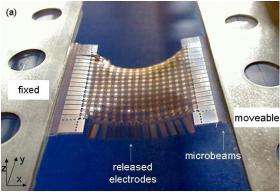
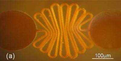
Among their experiments, the researchers constructed a network that consists of 5,041 micronodes with diameters of about 200 micrometers (these can host tiny sensors, actuators, etc.) that are connected in a grid-like pattern by microwires. The key to the expandable design is arranging the pre-expanded microwires in loops and segments - essentially, compressing as long a wire as possible between nodes in such a way to allow expansion at low strain levels. By coating the microwires with an aluminum layer, the researchers could enable them to function as electrical interconnects between the nodes for various electronic devices. Micronodes located on the periphery of the network could then relay electric signals into and out of the network.

The fabrication and expansion of the network is novel yet relatively straightforward. The researchers first patterned the functional microwires and micronodes (in the pre-expanded configuration) onto a 10-centimeter-diameter Kapton film, which is a polymer material that is also used as insulation for space suits and electrical wires in space shuttles. Unnecessary material was then removed from the Kapton film to form a network of micronodes interconnected by microwires.
The polymer network was then stretched by a hand-controlled stretching machine, first in one direction and then in the other. As the network expands, the microwire loops spread apart like an accordion (but the nodes don’t stretch). Using a microscope, the researchers inspected the expanded one-square-meter network and found that the microwires and micronodes were still mechanically and electrically sound. The micronodes were also precisely placed in predefined locations after expansion.
“The approach that I proposed is conceptually simple but nobody thought about it before,” Lanzara said. “Instead of trying to ‘stretch’ a material to cover large areas and rely only on the material’s physical properties, why not simply ‘remove unnecessary material’ from a polymer film and ‘engineer’ the remaining material in the shape of folded microwires and micronodes? In this way, by simply unfolding the microwires, the engineered material can be expanded to several orders of magnitude of its original size at very low strain values. This design leads to bidimensional stretching ratios that go beyond the stretching capability of any material known today.”
Overall, the expanded network is basically a macro-scale version of the centimeter-sized network, with both made of the same micro-sized components. In addition, the entire large network could be rolled up into various 3D shapes due to its high flexibility and could be easily integrated into materials of different rigidities such as flexible polymers and carbon fiber composites.
As the researchers explain, the highly expandable network can serve as a cost-effective way to integrate a high-density array of nano/micro-scale devices at the macro-scale level. While the primary application for this network may be for sensors that span large areas, the approach could also have applications in portable electronic equipment, paper-like displays, intelligent electronic textiles, and more.
“This work can certainly pave the way to space, civil, military, medical and biomedical applications as well as to the development of products which have the potential to enhance the comfort and quality of our lifestyle,” Lanzara said. “For instance, the expanded web can be used to realize smart textiles for clothing or for medical devices, to realize the morphing materials of the future, or multifunctional, exceptionally durable, reliable composites for safe and durable aircrafts as well as to realize the artificial skin of humanoid robots. Fabricating the network at the micro-scale and expanding it to the macro-scale in a single step allows for a drastic reduction of the integration costs into materials or structures, thus, the above mentioned applications can finally be practically realized.”
More information: G. Lanzara, J. Feng, and F-K Chang. “Design of micro-scale highly expandable networks of polymer-based substrates for macro-scale applications.” Smart Mater. Struct. 19 (2010) 045013 (18pp). Doi:10.1088/0964-1726/19/4/045013
Copyright 2010 PhysOrg.com.
All rights reserved. This material may not be published, broadcast, rewritten or redistributed in whole or part without the express written permission of PhysOrg.com.


