April 23, 2010 report
IBM demonstrates nonoscale 3D patterning technique (w/ Video)

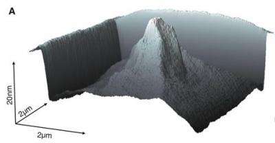
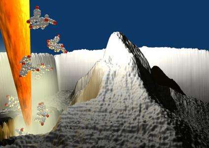
(PhysOrg.com) -- IBM Research in Zurich has demonstrated a new nanoscale patterning technique that could replace electron beam lithography (EBL). The demonstration carved a 1:5 billion scale three-dimensional model of the Matterhorn, a 4,478 meter high mountain lying on the border between Italy and Switzerland, to show how their technique could be used for a number of applications, such as creating nanoscale lenses on silicon chips for carrying optical circuits at a scale so small that electronic circuits are inefficient.
EBL (also called e-beam lithography) uses a focused beam of electrons to etch micro- or nano-scale patterns into a substrate covered by a film (the resist) that is sensitive to the electrons. It was initially developed for fabricating integrated circuits.
The 25-nanometer (nm) high model of the mountain was sculpted in around three minutes from a glassy organic material using a 500-nm long and 5-nm thick silicon scanning probe heated to above 330°C for a few microseconds — long enough to break hydrogen bonds within the material without breaking other bonds. The probe was fixed to a flexible cantilever that can scan the substrate to an accuracy of 1 nm. The probe acts like a microscopic milling machine removing layers of the substrate by heat and force.
The demonstration also sculpted a relief map of the world that measured 22 by 11 micrometers. According to the IBM press release the scale of the map is so small 1,000 of them could be drawn on a single grain of salt. IBM says the current technology can go as small as 15 nanometers, but in the future could go even smaller.
At that scale IBM’s technique could replace EBL, which costs 80 to 90% more and is slower. According Michel Despont, an IBM physicist and co-author of the research paper, the technique needs fewer processes than EBL, and the fact that it can be used to create structures in 3D means it could be used for applications no one has yet considered.
In their paper, published in the Science journal, the IBM researchers say they plan to use the technique to create meta-materials, optical components, for prototyping CMOS nanoelectronics components, and for making templates for nanorod or nanotube self-assembly. Despont said the system would not be commercially available for around five years, but they hope to make it available for universities and research laboratories before then.

More information:
Nanoscale Three-Dimensional Patterning of Molecular Resists by Scanning Probes, David Pires et al., Published Online April 22, 2010
Science DOI:10.1126/science.1187851
© 2010 PhysOrg.com


