May 20, 2010 report
New method to make gallium arsenide solar cells

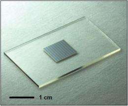
(PhysOrg.com) -- A new "transfer-printing" method of making light-sensitive semiconductors could make solar cells, night-vision cameras, and a range of other devices much more efficient, and could transform the solar industry.
Scientists at the University of Illinois at Urbana-Champaign have developed a new and cheaper way of producing microchips of gallium arsenide (GaAs), a compound semiconductor that responds to light. Gallium arsenide is about twice as effective as silicon in converting incident solar radiation to light, with a theoretical conversion rate of up to 40 percent, and has for that reason been used in solar cells in space crafts.
The problem with GaAs is its expense and the need for wafers to be grown in precisely controlled conditions. The wafers are sliced for use, but only the surfaces are used and the rest is essentially wasted. Now the Illinois research team, led by materials scientist John Rogers, has developed an alternative and potentially much more cost-effective technique involving growing stacks of layers of GaAs alternating with aluminum arsenide (AlAs).
When the stack is complete, the scientists then chemically etch away the AlAs layers using hydrofluoric acid, leaving the films of GaAs, which they then peel off and stamp onto another substrate such as glass, silicon, or plastic using a silicon-based soft rubber stamp. Rogers and his colleagues have been working on perfecting the technique for around ten years.

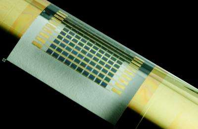
They have learned that if they press the stamp on the stack and lift it quickly it picks up only the top film. They then transfer the GaAs to the substrate by stamping it onto the surface and peeling the stamp back slowly. They could then build the devices such as photovoltaic cells, semiconductor field effect transistors and logic gates, and near-infrared imaging devices on the substrates. The method yields large quantities of high quality GaAs films, leaving the original wafer for reuse to grow more films.
Using their technique, which is described in the journal Nature, the researchers succeeded in mass-producing tiny solar cells about 500 micrometers in diameter, and they also produced components for mobile phones and infrared-imaging devices.
Rogers said GaAs has a great deal of potential in the future, and the team is now developing commercially viable solar cells that will be able to generate electricity for about $1 per watt.

More information: Jongseung Yoon, GaAs photovoltaics and optoelectronics using releasable multilayer epitaxial assemblies, Nature, Volume: 465, Pages: 329-333, Date published: 20 May 2010, DOI:doi:10.1038/nature09054
© 2010 PhysOrg.com


