X-Ray Vision: seeing plastic mixtures inside and out
(PhysOrg.com) -- Two scientists working in Europe have paved the way for improved plastic electronics by devising a technique that can be used to take images of plastic mixtures on the nanoscale simultaneously in the body of the material and at the surface.
Low-cost plastic solar cells, brighter displays, and a longer battery life for mobile phones and e-readers are some foreseeable outcomes, as manufactures could use the method to better understand the materials they use.
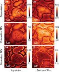
Chris McNeill of the University of Cambridge (UK) and Ben Watts of the Paul Scherrer Institute (Switzerland) are the researchers behind the breakthrough published in Macromolecular Rapid Communications. They shine synchrotron radiation on polymer mixtures to take sophisticated multiwavelength X-ray images of the bulk of the polymer mixture, and at the same time collect the electrons formed by the interaction of the X-rays with the surface of the sample. The second image can be compared directly with the first to see the differences in distribution of the components in the body of the film and on the surface.
The surface-imaging part works because any photoelectrons formed in the bulk of the material are absorbed before they reach the surface, and hence only those formed at the surface are free to leave the material and create a signal, which is “small, but measurable”.
Watts explains that “the X-rays that are shone on the sample are “tuned to the carbon atom”, causing the polymers, which are mostly carbon, to “resonate in a way that makes them absorb much more of the light at particular wavelengths than one would otherwise expect. This resonance between the light and atom is also very sensitive to the way in which the atoms are linked together... resulting in [high] contrast between polymer materials that otherwise appear nearly identical.” An example is shown in the picture.
“At Cambridge we are interested in the use of semiconducting polymers for applications in solar cells, light-emitting diodes (LEDs), and transistors,” says McNeill. “As is the case in other areas of polymer science, the blending of two semiconducting polymers sometimes enables you to achieve properties or function that cannot be achieved with the one polymer alone. The efficiency of polymer solar cells and LEDs are greatly improved through blending, and we are particularly interested in how film microstructure affects device performance. Being able to image not only bulk structure but surface structure as well is critical, as it is the surfaces that connect to the electrodes (and the outside world) so having a technique that helps us to understand how surface and bulk structures are connected was highly desirable.”
Both scientists studied in same group in Australia before going separate ways; McNeill to pursue his interest in organic semiconductors, and Watts his in synchrotron-based characterization. Their expertise in complementary areas meant they were abreast of current issues in the field of plastic electronics while being aware of new opportunities for advanced materials characterization.
McNeill: “In a sense all the components required for such an experiment have been available for a while, and it required a realization of this opportunity and the assembly of the components. We acknowledge Rainer Fink of the Universität Erlangen-Nürnberg for first demonstrating the feasibility of the experiment…There were some technical challenges in having to suppress the photoelectrons being emitted from other parts of the experiment in order to detect only those coming from the sample, but these were overcome mostly through Ben’s dogged persistence and thoroughness.”
They see the work as benefiting not just those working with semiconducting polymers, which are necessary for plastic electronics, but all types of thin-film polymer blends. There may also be applications in other organic, but non-polymer, mixtures or other materials where “characterization of surface and bulk is crucial.”
The next steps involve extending the analysis of surface structure to “a full quantitative analysis”, according to McNeill, “This would require imaging at multiple X-ray photon energies.” But the longer exposure times requires could damage the surfaces being studied. “We are also applying our technique to the study of polycrystalline semiconducting polymer films that will provide insight into the interplay between film microstructure and charge transport in these devices.”
More information: Macromol. Rapid Commun. 2010, DOI:10.1002/marc.201000269
Provided by Wiley


