15,000 beams of light: Pens that write with light offer low-cost, rapid nanofabrication capabilities

(PhysOrg.com) -- One Chicago skyline is dazzling enough. Now imagine 15,000 of them.
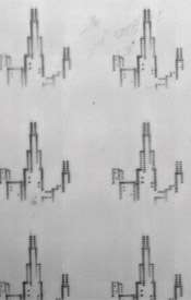
A Northwestern University research team has done just that -- drawing 15,000 identical skylines with tiny beams of light using an innovative nanofabrication technology called beam-pen lithography (BPL).
Details of the new method, which could do for nanofabrication what the desktop printer has done for printing and information transfer, will be published Aug. 1 by the journal Nature Nanotechnology.
The Northwestern technology offers a means to rapidly and inexpensively make and prototype circuits, optoelectronics and medical diagnostics and promises many other applications in the electronics, photonics and life sciences industries.
"It's all about miniaturization," said Chad A. Mirkin, George B. Rathmann Professor of Chemistry in the Weinberg College of Arts and Sciences and director of Northwestern's International Institute for Nanotechnology. "Rapid and large-scale transfer of information drives the world. But conventional micro- and nanofabrication tools for making structures are very expensive. We are trying to change that with this new approach to photolithography and nanopatterning."
Using beam-pen lithography, the researchers patterned 15,000 replicas of the Chicago skyline (featuring the Willis Tower and the John Hancock Center) simultaneously in about half an hour. Fifteen thousand tiny pens deposit the skylines over square centimeters of space. Conventional nanopatterning technologies, such as electron-beam lithography, allow one to make similarly small structures but are inherently low throughput and do not allow one to do large-area nanofabrication.
Each skyline pattern is made up of 182 dots, with each dot approximately 500 nanometers in diameter, like each pen tip. The time of light exposure for each dot was 20 seconds. The current method allows researchers to make structures as small as 150 nanometers, but refinements of the pen architecture likely will increase resolution to below 100 nanometers. (Although not reported in the paper, the researchers have created an array of 11 million pens in an area only a few centimeters square.)
Beam-pen lithography is the third type of "pen" in Mirkin's nanofabrication arsenal. He developed polymer-pen lithography (PPL) in 2008 and Dip-Pen Nanolithography (DPN) in 1999, both of which deliver chemical materials to a surface and have since been commercialized into research-grade nanofabrication tools that are now used in 23 countries around the world.
Like PPL, beam-pen lithography uses an array of tiny pens made of a polymer to print patterns over large areas with nanoscopic through macroscopic resolution. But instead of using an "ink" of molecules, BPL draws patterns using light on a light-sensitive material.
Each pen is in the shape of a pyramid, with the point as its tip. The researchers coat the pyramids with a very thin layer of gold and then remove a tiny amount of gold from each tip. The large open tops of the pyramids (the back side of the array) are exposed to light, and the gold-plated pyramids channel the light to the tips. A fine beam of light comes from each tip, where the gold was removed, exposing the light-sensitive material at each point. This allows the researchers to print patterns with great precision and ease.
"Another advantage is that we don't have to use all the pens at once -- we can shut some off and turn on others," said Mirkin, who also is professor of medicine and professor of materials science and engineering. "Because the tops of the pyramids are on the microscale, we can control each individual tip."
Beam-pen lithography could lead to the development of a desktop printer of sorts for nanofabrication, giving individual researchers a great deal of control of their work.
"Such an instrument would allow researchers at universities and in the electronics industry around the world to rapidly prototype -- and possibly produce -- high-resolution electronic devices and systems right in the lab," Mirkin said. "They want to test their patterns immediately, not have to wait for a third-party to produce prototypes, which is what happens now."
More information: The title of the Nature Nanotechnology paper is "Beam-pen Nanolithography."
Provided by Northwestern University


