Toshiba and NEC Develop Key Technologies for High-Density MRAM
Toshiba Corporation and NEC Corporation today announced two key advancements toward development of a magnetoresistive random access memory, a technology seen as key to the development of future generations of high performance mobile equipment. Unveiling the latest fruits of a joint development program dating back to 2002, the two companies announced a new cell design that halves power consumption during data writes and cuts writing errors, and a novel MRAM architecture with high speed characteristics and a performance that will support development of high-density devices.
Full details of the new technology were presented on December 14 at IEDM (International Electron Devices Meeting) 2004 in San Francisco, USA.
The features of MRAM are fast read/write, high density, unlimited endurance and non-volatility?the ability to retain data when switched off. While MRAM show great promise for application in mobile information equipment, cell size and power consumption must be reduced, and no loss of operating speed achieved, before commercial application is possible. The advancements reported by NEC and Toshiba point the way forward.
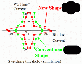
NEC and Toshiba reduced write current by developing a new shape for the magnetic tunneling junction (MTJ) that stores information in the cell. The MTJ shape is similar to the standard rectangular shape, but with arc-shaped bulges on both sides, in the middle of the longer length. Seen from above, the outline of the shape resembles a coin placed on a rectangle. With this new design, write current is approximately half that of present MRAM, and writing errors are reduced, even if there is some fluctuation in the switching characteristics of each memory cell. (Please refer to the figure 1.)
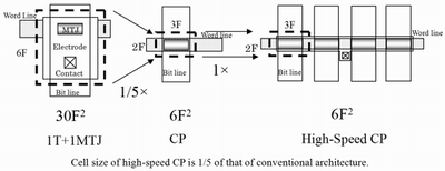
Toshiba and NEC have also developed highly promising new cell architecture. Research to date has produced two basic proposals on MRAM cell structure. The first of these couples each cell with a transistor, which advances read times, but at a cost in increased cell size. The second, the cross point (CP) structure, removes the transistor from each individual cell, a move that reduces cell size, but read access time gets longer and read errors occur due to generation of sneak current, the tendency of current to be directed to the unselected cell. Toshiba and NEC have realized a high-speed CP cell structure that uses one transistor to control four cells. This achieves a cell that is the same size as a standard DRAM cell and conventional CP cell, and much smaller than an MRAM cell with transistor. (Please refer to figure 2.) The new architecture also achieves a 250 nanosecond read time, four times faster than the conventional CP cell structure.
Through continued joint development, Toshiba and NEC aim to define fundamental technologies required for realizing a 256 megabit MRAM, utilizing MTJ based on 250 nanometer design rule and CMOS technologies based on 130-180 nanometer design rules by fiscal year 2005.
Development of the new MRAM technologies was supported by grants from Japan's New Energy and Industrial Technology Development Organization (NEDO).


