Matsushita Develops the AlGaN/GaN Power FET on Silicon Substrate
Matsushita's novel technology achieves a low-cost, low-loss fast switching device with 1/10 on-state resistance of Si power MOS
Matsushita Electric Industrial Co., Ltd., best known for its Panasonic brand products, today announced the development of a new transistor to revolutionize switching devices. The new transistor can be used as a low-loss power switching device in applications like inverters for home electric appliances, hybrid cars and switching power supplies.
The AlGaN/GaN power FET is an aluminum gallium nitride (AlGaN)/gallium nitride (GaN) field effect transistor (FET) fabricated on an inexpensive silicon. The transistor uses Panasonic's own crystal growing technology and GaN materials that have over 10 times the breakdown voltage and below 1/5 lower resistance of existing silicon (Si). As a result, it has achieved a 350 V breakdown voltage, same as Si power metal-oxide-semiconductors (MOS), a very low specific on-state resistance of 1.9 m Ohm cm2 (below 1/10 of Si power MOS), and high-speed power switching of less than 0.1 nanosecond (below 1/100 of Si power MOS). The transistor also has a current handling capability of 150 A (over five times that of Si power MOS).
Just one of these new transistors can substitute more than 10 parallel-connecting Si power MOSFETs, contributing significantly to power savings and miniaturization of electronic products. By adopting silicon substrates, the material cost is drastically reduced to less than 1/100 of silicon carbide (SiC) power MOSFETs.
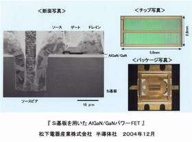
The new AlGaN/GaN power FET is the result of development of Panasonic's source-via-grounding (SVG) structure technology where the transistor source electrode is connected to the Si substrate through holes formed on the surface side. This eliminates source wires, bonding and pads from the substrate surface. Consequently, the chip size and wire inductance are significantly reduced.
An AlN/AlGaN buffer layer grown at a high temperature and an AlN/GaN multi-layer film are used on the first layer to reduce defect density on the Si substrate and improve the heterojunction interface quality. Panasonic developed the GaN growth technology in partnership with Professor Takashi Egawa of the Research Center for Nano-Device and System, Nagoya Institute of Technology. The new technology has been vital in making the new high power AlGaN/GaN FET.
By successfully growing GaN on an Si substrate, Panasonic responded, for the first time in the world, to the needs for low-loss switching devices that combine both high breakdown voltage and low specific on-state resistance. It was becoming increasingly difficult for current Si power MOSFETs to fulfill the needs.
Matsushita Electric Industrial Co., Ltd. has applied for 39 patents in Japan and 26 patents overseas on the new transistor.
The results of this development will be presented at the International Electron Devices Meeting (IEDM) 2004 held in San Francisco from December 13 to 15, 2004.


