Nanoscale electron island could lead to new efficient flat-panel displays
UW-Madison Electrical and Computer Engineering Associate Professor Robert Blick and colleagues in Germany have demonstrated a new nanoscale mechanism for field emission that could lead to a new type of energy efficient flat-panel display. The team's article in Physical Review Letters describes how a nanoscale gold-tipped island is able to mechanically oscillate between two facing electrodes, which provide recharging and detection of the emission current. Additionally, unlike many nanoscale experiments in field emission, the device does not need to be cryogenically cooled.
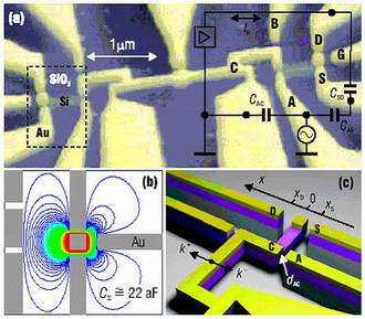
Image caption: see below.
Field emission, also called Fowler-Nordheim tunneling, is the process in which electrons tunnel through a barrier in the presence of a high electric field. This quantum mechanical tunneling process is an important mechanism for thin barriers such as those in metal-semiconductor junctions on highly-doped semiconductors. With its nanoscale device, the team is able to trace and reproduce the transition from current flow through a rectangular tunneling barrier to the regime of field emission.
"Field emission from microscopic tips has been a fundamental tools of experimental physics for decades, and nanoscale emitters are the subject of intense research" explains Blick. "However, contrary to earlier observed deviation from the Fowler-Nordheim, our isolated nanomechanical pendulum shows new behavior already at low voltages. The fact that the emitter is isolated alters the Fowler-Nordheim description to a behavior which becomes linear for large voltages."
The team will continue its research with the goal of understanding how field emission is performed in a controlled fashion, one electron at a time.
Image caption: (a) SEM micrograph of the device with two nanomechanical diodes. The right hand shuttle cantilever C is seen with gates A through S. The equivalent circuit of the setup is superimposed: the ac voltage is applied to gate A where it couples via CAS to the source S. The island is excited via the resulting resonant Coulomb force, and transferred electrons are detected at drain D. The amplifier's output is recorded vs frequency f of the ac voltage. (b) Finite element simulation of the electrostatic potential for a charged island and grounded surrounding. The island's overall capacitance C = 22 aF determines the energy required for charge transfer to the island. (c) Schematic of the nanomechanical diode featuring geometrical details and definitions, including the mechanical asymmetry of the spring constant k. The metallic island dimensions are 80x80x50 nm3.
Source: University of Wisconsin-Madison


