Devising nano vision for an optical microscope

February 10, 2005 nano vision for an optical microscope

Contrary to conventional wisdom, technology's advance into the vanishingly small realm of molecules and atoms may not be out of sight for the venerable optical microscope, after all. In fact, research at the National Institute of Standards and Technology (NIST) suggests that a hybrid version of the optical microscope might be able to image and measure features smaller than 10 nanometers--a tiny fraction of the wavelength of visible light.

In a preliminary test of the embryonic technique, NIST scientists used violet light with a wavelength of 436 nanometers to image features as small as 40 nanometers, about five times smaller than possible with a conventional optical microscope.

Roughly speaking, such a feat is akin to picking up a solitary dime with a clumsy front-end loader. If successfully developed, the imaging technology could be readily incorporated into chip-making and other commercial-scale processes for making parts and products with nanometer-scale dimensions.

The wavelengths of light in the visible part of the spectrum greatly exceed nanoscale dimensions. Consequently, the resolution of conventional light-based imaging methods is limited to about 200 nanometers--too large to resolve the details of nanotechnology, which, by definition, are no more than half that size.

However, a newly begun, five-year research effort at NIST suggests that a novel combination of illumination, detection and computing technologies can circumvent this limitation. Success would extend the technology's 400-year-long record as an indispensable imaging and measurement tool well into the expanding realm of nanotechnology.

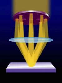
Called phase-sensitive, scatter-field optical imaging, the computer-intensive technique under development at NIST uses a set of dynamically engineered light waves optimized for particular properties (such as angular orientation and polarization). How this structured illumination field--engineered differently to highlight the particular geometry of each type of specimen--scatters after striking the target can reveal the tiniest of details.

"The scattering patterns are extremely sensitive to small changes in the shape and size of the scattering feature," explains Rick Silver, a physicist in NIST's Precision Engineering Division.


Rate this story - not rated yet


February 10, 2005 all stories

Comments: 0

not rated yet

  • hide
  • Related Stories

  • Small nanoparticles bring big improvement to medical imaging
    created Nov 18, 2009 | popularity not rated yet | comments 0
  • LIDAR system offers peerless precision in remote measurements
    created May 24, 2009 | popularity not rated yet | comments 0
  • Cold atoms could replace hot gallium in focused ion beams
    created Nov 13, 2008 | popularity not rated yet | comments 0
  • Nanoscale Dimensioning Is Fast, Cheap with New Optical Technique
    created Oct 29, 2008 | popularity not rated yet | comments 0
  • Gold Nanostars Outshine the Competition
    created Oct 15, 2008 | popularity not rated yet | comments 0


Other News

Scientists discover novel materials approach to fighting cancer (w/ Video)

Nanotechnology / Bio & Medicine

created 21 hours ago | popularity 4.7 / 5 (6) | comments 0 | with audio podcast

(PhysOrg.com) -- Scientists from the U.S. Department of Energy's Argonne National Laboratory and the University of Chicago Medical Center are shaking up the world of materials science and cancer research on the cover of the ...


Spray-on liquid glass

Spray-on liquid glass is about to revolutionize almost everything

Nanotechnology / Nanomaterials

created Feb 02, 2010 | popularity 4.7 / 5 (236) | comments 93 | with audio podcast report

(PhysOrg.com) -- Spray-on liquid glass is transparent, non-toxic, and can protect virtually any surface against almost any damage from hazards such as water, UV radiation, dirt, heat, and bacterial infections. ...


IBM Scientists Demonstrate World's Fastest Graphene Transistor

IBM Scientists Demonstrate World's Fastest Graphene Transistor

Nanotechnology / Nanophysics

created Feb 05, 2010 | popularity 4.9 / 5 (38) | comments 23 | with audio podcast

(PhysOrg.com) -- In a just-published paper in the magazine Science, IBM researchers demonstrated a radio-frequency graphene transistor with the highest cut-off frequency achieved so far for any graphene device ...


Conductive eTextiles: Stanford finds a new use for cloth

Conductive eTextiles: Researchers move from making batteries from paper to making batteries from cloth

Nanotechnology / Nanomaterials

created Feb 05, 2010 | popularity 4.3 / 5 (7) | comments 4 | with audio podcast

(PhysOrg.com) -- Stanford researchers have moved from making batteries from paper to making batteries from cloth. Your-T-shirt could become a lighted, moving display.


Carbon Based Chips May One Day Replace Silicon Transistors

Carbon Based Chips May One Day Replace Silicon Transistors

Nanotechnology / Nanomaterials

created Feb 03, 2010 | popularity 4.7 / 5 (17) | comments 3 | with audio podcast weblog

(PhysOrg.com) -- IBM researchers are hopeful that, over the next decade, silicon-based transistors will be replaced by carbon-based transistors. IBM has already laid out the ground work for carbon-based transistors.