Nanotech advance makes carbon nanotubes more useful
Researchers at UCSD have made carbon nanotubes bent in sharp predetermined angles, a technical advance that could lead to use of the long, thin cylinders of carbon as tiny springs, tips for atomic force microscopes, smaller electrical connectors in integrated circuits, and in many other nanotechnology applications. In a paper published in the April 7, 2005, issue of the Journal of Physical Chemistry B, Sungho Jin, a professor of materials science at UCSD’s Jacobs School of Engineering, reported a technique to create bent nanotubes by manipulating the electric field during their growth and adjusting other conditions.
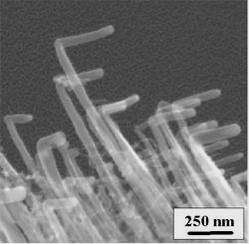
Image: UCSD researchers exploited the strong alignment of nanotube growth with the direction of electric field lines to create tailor-made bends.
"Controlling nanotube geometry is necessary to realize the many promised applications of these materials," said Jin, a professor in the Jacobs School’s Department of Mechanical and Aerospace Engineering. “Our new results show that we have taken a step toward understanding how to shape nanotubes to our specifications, an achievement that could greatly enhance their value to society.”
Joseph AuBuchon, a graduate student in Jin’s group, exploited the strong alignment of nanotube growth with the direction of electric field lines. After growing an aligned array of straight nanotubes, AuBuchon switched the orientation of electric field lines 90 degrees to make L-shaped tubes. He then made more orientation changes to make zigzags. AuBuchon won a Gold Graduate Student Award and Best Poster Award for presenting details of his nanotube research at the spring 2005 meeting of the Materials Research Society, which was held March 28‑April 1 in San Francisco.

Carbon nanotubes hold great promise because of their exceptionally strong mechanical properties, their ability to efficiently carry high densities of electric current, and other unique electrical and chemical properties. AuBuchon used a plasma enhanced chemical vapor deposition technique to grow about 2 billion nanotubes per square centimeter on silicon wafers seeded with nickel catalyst nanoparticles.
Nanotubes, which are roughly 10,000 times smaller than a human hair, can be made almost perfectly straight in special chambers of gas plasma. Successfully shaping nanotubes has been a goal of materials scientists since a Japanese researcher discovered them in 1991. However, the creation of sharp bends is difficult because once a growth phase of nanotubes is interrupted, the catalyst particles at the tips of the growing nanotubes become encased with carbon, blocking future growth. A key to Jin and AuBuchon’s successful growth of bent nanotubes involved the discovery of a technique to prevent the unwanted carbon from encasing the catalyst between growth steps.
“It’s hard to imagine all the possible uses for bent nanotubes, but we think one of them might be to improve the performance of atomic force microscopy,” said Jin. Atomic force microscopy uses a mechanical probe to magnify rigid materials at the atomic scale to produce 3-D images of the surface.
Jin also noted that nanotubes may be used as replacements for conventional electrical connectors made of metal wires in ever smaller integrated circuits. Such wires are roughly 70 nanometers wide, but nanotube connectors as thin as 1.2 nanometers are theoretically capable of supplying sufficiently large electric currents to integrated circuits.
In addition, Jin said the interconnections between microcircuit devices are often made with metal alloy solders. Unfortunately, these solders expand and contract at rates different than those of the microcircuit device, and cycles of heating and cooling cause fatigue cracking at interconnections. “If these interconnections were made with electrically conducting nanotube zigzags, which also act as springs, not only would we need much less space to make these interconnections, but the thermal-expansion mismatch also wouldn’t matter because the interconnections are flexible,” says Jin. “We call it the compliant nano-interconnect.”
Using a modification of the approach to make zigzag nanotubes, Jin and AuBuchon also produced parallel arrays of T- and Y-shaped nanotubes that could be used to make fuel cells more efficient. These arrays of parallel, branched nanotubes could act as a 3-D scaffolding for platinum catalyst particles. High densities of platinum catalyst-tipped nanotubes could enable fuel cells produce electricity more efficiently.
Source: University of California - San Diego


