The nano-revolution continues at Argonne
Federal and state officials will visit Argonne National Laboratory May 6 to participate in a cornerstone-laying ceremony for the Center for Nanoscale Materials (CNM).
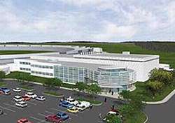
The CNM, which is currently under construction, is a joint DOE-State of Illinois project to provide basic nanoscale research that will lead to industrial and commercial applications that can benefit Illinois and the country.
Image: Artist's conception of the Center for Nanoscale Materials now under construction at Argonne.
"Nano" refers to the scale used to measure these materials – a nanometer is 1 billionth of a meter, or about 70,000 times smaller than the width of a human hair. Materials at the nanoscale differ from conventional materials because traditional physics does not apply at this scale.
“Intentionally building materials at the nanoscale,” said CNM Director Eric Isaacs, “allows us to explore and develop entirely new ways to tailor a material's response to temperature, electrical or magnetic fields, or chemical environments. The basic research to be conducted at the CNM is critical so that novel, environmentally safe products and applications can be effectively developed based on nanomaterials.”
Industry will be able to use research revealed by CNM researchers to understand what can be expected from nanoscale materials. They will be able to create new products that will impact the fields of energy, medicine, information technology and homeland security, and to maintain the United States' leading role in science.
The center's mission includes supporting basic research and development of advanced instrumentation for creating novel materials that provide new insights at the nanoscale level. The challenges involve fabricating and exploring novel nanoscale materials and, ultimately, employing unique synthesis and characterization methods to control and tailor nanoscale phenomena.
The CNM will be open to academia, industry and other government laboratories through a peer-reviewed process.
CNM's research facilities
The facility is being built adjacent to the Advanced Photon Source, the most brilliant source of research X-rays in the Western Hemisphere. The 85,000-square foot CNM building will house research instruments, laboratories, clean rooms and work space to assist in fabricating and understanding these tiny materials.
CNM's first dedicated instrument will be the pioneering nanoprobe beam line now under construction. The nanoprobe will be a hard X-ray microscopy beamline with the highest spatial resolution in the world. With its combination of fluorescence, diffraction and transmission imaging at a spatial resolution of 30 nanometers or better in a single tool, the nanoprobe will be able to penetrate samples in situ and provide information about their internal structures.
An electron-beam lithography facility will provide fabrication support to CNM users, including a 100-kilovolt electron-beam lithography tool – one of a handful of such devices in the country. The center will also feature an Argonne-developed nanopositioning system for precision motion and measurement.
The CNM is a joint partnership between the Department of Energy and the State of Illinois. The State of Illinois is providing $36 million to construct the building, and DOE is providing an additional $36 million to develop and build the facility's advanced instrumentation.
Argonne's CNM is one of five centers being built at national laboratories across the country as part of DOE's Nanoscale Science Research Center program under the Office of Basic Energy Sciences.
The basic scientific research to be conducted at the CNM is predicted to lead to novel, environmentally safe products and applications that can be effectively developed based on nanomaterials. Research includes:
-- Nanomaterials that could lead to 400 percent improvement in the efficiency of direct conversion of heat to electricity, and conversely in thermoelectric cooling.
-- New materials to efficiently harvest light for energy generation, and for novel purposes such as selective chemical reactivity.
-- The means to synthesize and understand new nanostructured materials that are potentially stronger, lighter, harder, safer and self-repairing such as nanocarbon, which has led to coatings for implantable biomedical devices such as an artificial retina.
-- Developing advanced, adaptive biosensors, for instance, to monitor blood sugar levels and inject insulin directly into the blood stream.
-- Fundamental understanding and design of novel nanoscale materials and chemical processes capable of capturing, converting and storing energy as electrical or chemical equivalents. These developments could lead to using energy to manipulate biological materials in processes such as gene surgery or cell repair, and facilitating conversion of light energy into therapeutic processes.
-- New ways to manipulate photons and electrons, making possible a whole new class of devices, including those based on the spin of the electron.
-- Nanomagnetic and nanostructured ferroelectric materials for semiconductors will provide a path that goes beyond current technology for information processing and storage. New materials and devices will be developed at the CNM that are capable of much higher storage densities that use less power and dissipate less heat.
-- Nanophotonics research is poised to manipulate light at length scales much smaller than is possible using traditional optical elements, firmly placing light within the realm of the integrated circuit.
-- Sensors to detect the presence of biowarfare agents, such as anthrax, in real time.
Link: Center for Nanoscale Materials
Source: Argonne National Laboratory


