Nanotechnology combined with superconductivity could pave the way for 'spintronics'
As the ever-increasing power of computer chips brings us closer and closer to the limits of silicon technology, many researchers are betting that the future will belong to "spintronics": a nanoscale technology in which information is carried not by the electron's charge, as it is in conventional microchips, but by the electron's intrinsic spin.
If a reliable way can be found to control and manipulate the spins, these researchers argue, spintronic devices could offer higher data processing speeds, lower electric consumption, and many other advantages over conventional chips—including, perhaps, the ability to carry out radically new quantum computations.
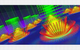
Image: The idea is to create the device as a series of layers, each only a few dozen nanometers thick. At the bottom is a layer of diluted magnetic semiconductor (DMS) material—for example, gallium arsenide doped with manganese atoms. Each manganese atom contributes an extra electron to the material, and thus an extra electron spin. Above that is a layer of insulator (grey) and then a layer of superconducting material (SC). Zooming in shows the magnetic field (green), which can thread through the superconducting layer only pinching itself down into an array of nanoscale flux tubes (green columns). The field in each flux tube is very intense, and extends right through the DMS layer. As it does, it forces a patch of electron spins to fall into line (red arrows). It also causes a certain amount of electric charge to accumulate (yellow). Credit: Dr. Ovidiu Toader, University of Toronto
Now, University of Notre Dame physicist Boldizsar Janko and his colleagues believe they have found such a control technique. Their work, funded by the National Science Foundation through a Nanoscale Interdisciplinary Research Team grant, was published in the March 5, 2005, edition of the journal Nature.
The idea is to create the device as a series of layers, each only a few dozen nanometers thick. At the base is a layer of diluted magnetic semiconductor, a type of material Janko and his group have been studying intensively. When gallium arsenide is doped with manganese atoms, for example, each manganese atom contributes an extra electron, and thus an extra electron spin; the result is a semiconductor material that can be magnetized in much the same way as iron. Then an insulator material is layered over the base, followed by a layer of superconducting material.
Next, a magnetic field is applied perpendicular to the top surface (see animation above). Thanks to the basic physics of superconductors, the field can make it through only by pinching itself down into an array of nanoscale flux tubes. That super concentrates the field inside each tube, so that it creates a spot of high-intensity magnetism on the semiconductor layer below, which, in turn, creates a patch of closely aligned electron spins. The resulting spin patches, one for each flux tube, are then available for encoding information.
The effect resembles what happens when you sprinkle iron filings on a piece of paper, and then hold a bar magnet underneath, says Janko: the presence of the magnet (the flux tube) makes the iron filings (the spins) stand at attention. Furthermore, he says, just as you can manipulate the filings by moving the magnet underneath the paper, you can manipulate the spins in this system by moving the flux tubes.
For example, an electric current flowing through the superconductor will cause a given flux tube to move to one side (with the patch of spins underneath moving along with it), while a current flowing in the reverse direction will move it back to the other side.
Although Janko and his colleagues have tested their approach so far only through computer simulations, experiments are now underway to demonstrate the technique in the laboratory.
Source: NSF


