Unexpected Results Lead To 'Nanocarbons': 'Flying' Nanotubes Are Strong And Hard
Diamonds are the hardest known substance. Carbon nanotubes are the strongest. Scientists at the U.S. Department of Energy's Argonne National Laboratory tried to combine the best of both worlds by creating a composite nanostructure. They wanted to grow tiny carbon tubes with tiny diamonds.
But the results were not as expected.
Instead, the experiment altered the surface area of the nanotubes, creating wing-like extensions. Even though the result wasn't what the experimenters were looking for, these modified surfaces may push nanotubes further into the world of practical and applied materials and systems. It also provides insight into how to synthesize an emerging class of material called “nanocarbons,” which consist of different allotropes — the same elements with different molecular structures — of carbon combined at the nanoscale to yield new materials with unique properties.
“We were trying to get a composite, but the nanotubes were becoming modified,” Argonne researcher Susan Trasobares said. “Who could have guessed?”
The carbon atoms that makes up nanotubes and fullerenes are bonded like graphite in sheets that resemble “chicken wire.” When the sheets are rolled into a ball they make fullerenes – the soccer-ball-shaped carbon molecules, different from both graphite and diamond. If the sheets are rolled into a seamless cylinder, they create carbon nanotubes.
The unique properties of these nanotubes, including their strength, electrical properties and conducting capabilities, make them useful in electronic and mechanical applications. And they are small — only one ten-thousandth the width of a human hair.
Carbon nanotubes have been used for structural reinforcement and in lithium-ion batteries and television screen displays, but Argonne scientist John Carlisle said they are still in the prototype stage.
Researchers are looking for ways to alter nanotubes' properties. Carlisle said that by growing diamonds and nanotubes together, he and Trasobares may get a composite structure that is better than the sum of the parts.
So, they stood the nanotubes up on their ends, like forks sticking up, and then put them under the plasma reactor. Since the plasma was usually used to grow ultrananocrystaline diamonds, a type of diamond film with nanometer grains, they thought diamonds would grow on the ends of the tubes.
“Well, it didn't work,” Carlisle said. “It was an abysmal failure. This is science at its best.”
The plasma ate away the ends of the nanotubes. The carbon reacted with the plasma and vaporized.
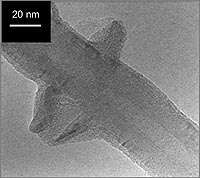
However, in one of the samples, some of the nanotubes were knocked into a horizontal position — like crop circles in the nanotube sample. After examining the samples with the help of the Electron Microscopy Center, the researchers discovered that the same etching process that destroyed the vertical nanotubes was simply ripping open the smooth side walls of the horizontal nanotubes. Then carbon molecules bonded to create wings.
Carlisle said he considered naming the modifications “prickly nanotubes” or “flying nanotubes,” but Trasobares suggested “graphitic wings” to describe these unique structures, and Carlisle agreed.
“The good part when you do research is that many times you find something you weren't expecting,” Trasobares said. “You have to ask: What's going on? What are we getting? Why are we getting it? What does it mean?”
For science, it means there is a new process to modify the smooth unreactive surface of the nanotubes, increasing the surface area and the number of reactive points. Most importantly the study breaks ground for new nanomaterials and new nanocomposites with new properties.
And researchers can speculate on possible applications.
As the number of reactive zones increases, the number of molecular groups that can attach to the nanotubes increases. Functionalization improves. The increase in surface area could also change electron emission properties, which are important for flat panel displays. More emission sites mean a larger current, which means a brighter display.
Wings could also help anchor the nanotube to polymers. The two rarely make a good connection. With this advance, the doors are opened for chemical sensors, probe tips, fuel cells, particle X-rays, fabrics, nanowires and artificial muscles.
As the research continues, more applications may be developed. But Carlisle said this won't happen overnight. There are still a lot of tests to do and a lot of problems to solve.
“As scientists, we dream about what things might be possible,” Carlisle said. “When you look at the process of how real technology develops, you begin to appreciate how really hard it is.”
Additional authors of the report, which was featured on the inside cover of Advanced Materials April issue, are Argonne's James Birrell and Dean Miller; Chris P. Ewels of the Composite Systems and Materials Department of the Office National d'Etudes et de Recherches Aerospatiales in France; Odile Stephan of Université Paris Sud; and Bingqing Q. Wei, Pawel Keblinski and Pulickel M. Ajayan of Rensselaer Polytechnic Institute.
The National Science Foundation, Rensselaer Polytechnic Institute, and the U.S. Department of Energy's Offices of Science and of Energy Efficiency and Renewable Energy supported the work.
The nation’s first national laboratory, Argonne National Laboratory conducts basic and applied scientific research across a wide spectrum of disciplines, ranging from high-energy physics to climatology and biotechnology. Since 1990, Argonne has worked with more than 600 companies and numerous federal agencies and other organizations to help advance America's scientific leadership and prepare the nation for the future. Argonne is operated by the University of Chicago for the U.S. Department of Energy's Office of Science.
Source: Argonne National Laboratory


