Brookhaven Scientists Create a New Nanostructure
Scientists from the U.S. Department of Energy's Brookhaven National Laboratory have devised a method to create a new, intriguing nanostructure: ultra-thin, ribbon-like "nanobelts" bound to nanotubes. Their research achieves several "firsts" in the field of nanoscience, the study of materials on the scale of a billionth of a meter. Additionally, the new structure, described in the June 4, 2005, online version of Nano Letters, is likely to have unique electrical and mechanical properties, and may be useful in many developing nanotechnologies.
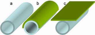
Image: The nanobelt-creation process. A nanotube (a) is coated with disorganized germanium atoms (b) that crystallize upon heating, resulting in a rigid germanium nanobelt bonded to the nanotube (c).
"We have produced nanobelts that have controllable thicknesses of about two to five nanometers. It is significant work, since the controllability, the thinness, and the methods we used are all new achievements," said Brookhaven materials scientist Wei-Qiang Han, the study's lead researcher. "But, we are most excited about creating a brand-new type of nanostructure."
To "grow" the nanobelts, which are made of the element germanium, Han and his colleagues first deposited nanotubes onto a grid surface made of copper. They used carbon nanotubes initially and later switched to boron-nitride nanotubes, which are very similar to the carbon variety.
Next, they coated the nanotubes with a disorganized, or "amorphous," layer of germanium atoms, which covered only the exposed top halves. The thickness of the layer was monitored with a device that can easily sense a change of just one-tenth of a nanometer.
Finally, they heated the germanium-coated nanotubes to 750 degrees Celsius inside a very powerful microscope. During heating, the amorphous germanium atoms crystallized and, simultaneously, pulled away from the sides of the nanotubes, changing from a curved half-cylinder to a rigid, flat strip about four nanometers thick. The nanobelts remained chemically attached to the nanotubes, resembling, for example, a ruler glued to the side of a cardboard tube.
"This method is much better than other techniques, which typically yield nanobelts more than 10 nanometers thick," said Han. "Achieving smaller thicknesses is important, since thinner nanobelts have physical properties — better conductivity, for example — that are more suitable for applications, such as components in nanoscale electronic circuits. Also, because our nanobelts are bound to nanotubes, they will likely possess different properties than stand-alone nanobelts or nanotubes. We believe this new structure will enable many new advances in nanotechnology."
In future research, Han and his colleagues plan to study the nanostructure's properties, such as its ability to transport electrons. Understanding how the structure conducts will help them determine if it may be used as a component in nano-electronic circuits.
Han's collaborators on this research are Myron Strongin of Brookhaven's Physics Department and Lijun Wu and Yimei Zhu, both of Brookhaven's Center for Functional Nanomaterials. The work was funded by the Office of Basic Energy Sciences within the U.S. Department of Energy's Office of Science.
Related Link: Brookhaven Center for Functional Nanomaterials
Source: Brookhaven National Laboratory


