New design developed for silicon nanowire transistors

July 1, 2005 New design developed for silicon nanowire transistors

In an advance for nanoscale electronics, researchers at the National Institute of Standards and Technology (NIST) have demonstrated a new design for silicon nanowire transistors that both simplifies processing and allows the devices to be switched on and off more easily.

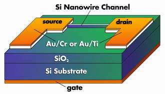
Image: A schematic diagram of the NIST nanowire transistor.

The NIST design, described in a paper published June 29 by the journal Nanotechnology,* uses a simplified type of contact between the nanowire channel and the positive and negative electrodes of the transistor. The design allows more electrical current to flow in and out of the silicon. The researchers believe the design is the first to demonstrate a "Schottky barrier" type contact for a nanowire transistor built using a "top-down" approach. This barrier, an easily formed metal contact that electrons can tunnel through, requires much less doping with impurities than do conventional ohmic contacts, thereby simplifying processing requirements. Schottky contacts also offer more resistance and restrict electrical flow to one direction when the transistor is off.

In the NIST transistor design, the 60-nanometer-wide channels exhibit a much greater difference in current between the on and off states than is true for larger reference channels up to 5 micrometers wide. This suggests that when a channel is scaled down to the nano regime, the ultra-narrow proportions significantly reduce the current leakage associated with defects in silicon. As a result, the transistors are less sensitive to electronic "noise" in the channel and can be turned on and off more effectively, according to the paper's lead author, Sang-Mo Koo, a NIST guest researcher.

Silicon nanowire devices have received considerable attention recently for possible use in integrated nanoscale electronics as well as for studying fundamental properties of structures and devices with very small dimensions. The NIST work overcomes some key difficulties in making reliable devices or test structures at nanoscale dimensions. The results also suggest that nanowire transistors made with conventional lithographic fabrication methods can improve performance in nanoscale electronics, while allowing industry to retain its existing silicon technology infrastructure.

*S.M. Koo, M.D. Edelstein, Q.Li, C.A. Richter and E.M. Vogel. 2005. Silicon nanowires as enhancement-mode Schottky barrier field-effect transistors. Nanotechnology 16. Posted online June 29.

Source: NIST


print this article email this article download pdf blog this article bookmark this article     Stumble it Digg this share on Facebook retweet share on Reddit add to delicious
Rate this story - 3.4 /5 (8 votes)


July 1, 2005 all stories

Comments: 0

3.4 /5 (8 votes)
  • Stumble this up

  • Digg this

  • share this

  • hide
  • Related Stories

  • ‘High Q’ Nanowires May be Practical Oscillators
    created Nov 27, 2007 | popularity not rated yet | comments 0
  • Silicon nanowires upgrade data-storage technology
    created Jun 09, 2007 | popularity not rated yet | comments 0
  • Placing single nanowires: NIST makes the connection
    created Apr 27, 2007 | popularity not rated yet | comments 0
  • Growing Glowing Nanowires to Light Up the Nanoworld
    created May 25, 2006 | popularity not rated yet | comments 0
  • New design for transistors powered by single electrons
    created Feb 02, 2006 | popularity not rated yet | comments 0


Other News

Fast, easy, and highly sensitive arsenic detection with gold nanoparticles

Nanotechnology / Nanomaterials

created 5 minutes ago | popularity not rated yet | comments 0

(PhysOrg.com) -- Mention of arsenic poisoning usually brings to mind underhanded murder. However, the danger of arsenic poisoning from contaminated drinking water is far greater. Low concentrations of arsenic are found in ...


Nanotech in Space: Experiment To Weather the Trials of Orbit

Nanotech in Space: Experiment To Weather the Trials of Orbit

Nanotechnology / Nanomaterials

created 12 hours ago | popularity 4 / 5 (2) | comments 0

Novel nanomaterials developed at Rensselaer were sent into orbit on Nov. 16 aboard Space Shuttle Atlantis.


Nanoparticles used in common household items caused genetic damage in mice

Nanotechnology / Bio & Medicine

created Nov 16, 2009 | popularity 4.8 / 5 (24) | comments 11

Titanium dioxide (TiO2) nanoparticles, found in everything from cosmetics to sunscreen to paint to vitamins, caused systemic genetic damage in mice, according to a comprehensive study conducted by researchers at UCLA's Jonsson ...


Water droplets direct self-assembly process in thin-film materials

Nanotechnology / Nanomaterials

created Nov 23, 2009 | popularity 5 / 5 (4) | comments 2

You can think of it as origami - very high-tech origami. Researchers at the University of Illinois have developed a technique for fabricating three-dimensional, single-crystalline silicon structures from thin films by coupling ...


Nanotube defects equal better energy and storage systems

Nanotube defects equal better energy and storage systems

Nanotechnology / Nanomaterials

created Nov 19, 2009 | popularity 4.4 / 5 (10) | comments 2

(PhysOrg.com) -- Most people would like to be able to charge their cell phones and other personal electronics quickly and not too often. A recent discovery made by UC San Diego engineers could lead to carbon ...