Integration of semiconductor and superconductor electronics on the nanoscale
In the July 8 issue of Science, scientists from the Kavli Institute of Nanoscience Delft and Philips present the first superconducting transistors based on semiconductor nanowires. These nanoscale superconductor/semiconductor devices enable the fabrication of new nanoscale superconducting electronic circuits and at the same time they provide new opportunities for the study of fundamental quantum transport phenomena.
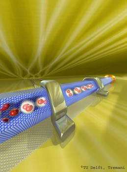
Image: Rendering of a semiconductor nanowire contacted by two superconducting metal electrodes. An opening in the side of the nanowire allows the viewer to look in the inside and see the conduction electrons. Close to the superconducting contacts the electrons are paired due to induced superconductivity, the main result of our work. The sky is formed by one of the measurements presented in the article. At the end of the nanowire the catalytic gold particle is located, a clear signature of the 'bottom-up' nature of the nanowires.
After the invention of the first solid-state transistor (Bardeen, Brattain and Shockley, 1947), semiconductors have become the reference material system for electronics. This success results from the possibility to control the resistance of a semiconductor with an electrical voltage applied to a nearby gate electrode. Despite the astonishing number of different types of semiconductor devices it has always been difficult to combine semiconductors with superconducting materials, i.e. materials with vanishing resistance at low temperatures. This exotic combination has captured the attention of both experimental and theoretical physicists already since the 80s. It enables new technology for electronic circuits based on dissipation-less superconducting elements which could be exploited for advanced applications where the requirement of low-temperature operation is not a limiting factor.
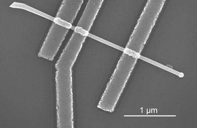
Image above: Scanning electron micrograph of one of the semiconductor nanowire devices. The nanowire is contacted by three superconducting aluminum contacts that induce the superconductivity in the nanowire. The device is fabricated on an oxidized doped silicon wafer that is used as a gate electrode in order to control the supercurrent. At the end of the wire the gold nanoparticle is clearly visible.
The results presented in the Science article show that the combination of indium arsenide semiconductor nanowires with aluminum-based superconducting contacts results in very reproducible superconducting transistors. In these devices a supercurrent (i.e. a current without resistance) can flow through the nanowire from one superconducting contact to the other. This quantum effect can be described as the “leakage” of Cooper pairs (i.e. paired electrons responsible for superconductivity) from the superconducting contacts into the semiconductor nanowire. Moreover, this supercurrent can be controlled by a gate voltage making it a supercurrent transistor.
The use of a recently developed method to grow semiconductor nanowires plays a central role in this achievement. The nanowires are made in a “bottom up” technology, i.e. instead of growing layers of material and removing the regions that are not needed, a device is constructed from small building blocks. In this case the nanowires grow from small gold particles by a vapor-liquid-solid (VLS) process. The size of these nanoparticles is in the range between 10 and 100 nm and this sets the diameter of the nanowires. The length of the nanowires is proportional to the growth time and can easily reach tens of microns providing a convenient aspect ratio for post-growth device fabrication.
The demonstrated high yield of the superconducting devices is an important requirement for the successful up scaling to small superconducting circuits incorporating multiple nanowire devices. For instance, two nanowire devices could be used to build an electrically tunable superconducting quantum interference device (SQUID). Such a device could be useful in solid-state quantum computer architectures as a switchable coupling element between superconducting quantum bits. Another possibility could be the combination of a nanowire light-emitting diode (LED; this can be made by alternating the semiconductor vapor between n- and p-doped during growth) with superconductivity in order to transfer quantum information from electrons to photons.


