New Infrared Tool Measures Silicon Wafer Thickness
In the last few years, semiconductor circuit features have shrunk to sub-100 nanometer dimensions, while the size of the thin silicon wafers that these circuits are constructed on has grown from 200 millimeters (mm) to 300 mm (about 12 inches). The payoff is a higher yield of finished devices from fewer wafers.
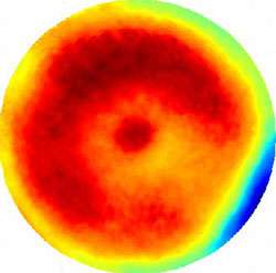
Image: A new NIST calibration system under development used infrared laser light to precisely measure the thickness of 300 millimeter silicon wafers. Changes in color within the spatial map above represent changes in wafer thickness. Green represents the average wafer thickness, while red, orange and yellow areas are thicker, and turquoise and blue areas are thinner. Credit: Q. Wang, U. Griesmann/NIST
The tough part, however, is to make wafers substantially larger while simultaneously meeting higher quality control specifications. The optics and materials for “printing” nanoscale circuit lines require that the wafers used are perfectly flat and of uniform thickness. To help the semiconductor industry meet its 2010 quality control roadmap goals, researchers at the National Institute of Standards and Technology (NIST) recently developed a new instrument that accurately measures differences in thickness across a 300 mm wafer with an excellent repeatability of 5 nm. The researchers hope the tool, with further refinements, will allow them to establish a new calibration service for “master wafers” used in the industry to measure wafer thickness.
The NIST researchers will describe the instrument, the Improved Infrared Interferometer, or IR3 for short, at a technical conference* in late July. Like all interferometers, the IR3 uses intersecting waves of light to create interference patterns, which in turn can be used as a ruler to measure nanoscale dimensions. While most interferometers use red laser light, the IR3 uses infrared laser light. And unlike visible light, these much longer wavelengths pass right through a silicon wafer. This means that IR3 can illuminate the top and bottom on a 300 mm wafer and produce a detailed spatial map of differences in thickness in one pass. Conventional tools require spinning the wafer and measuring at multiple locations.
The NIST researchers make precision measurements of the wafer’s index of refraction—the amount that light is “bent” as it passes through the silicon—as a critical step in correctly interpreting the interference patterns. Increased precision in the refractive index measurement will be necessary before “absolute” measurements of thickness rather than relative differences will be possible with the new instrument.
*Q. Wang, U. Griesmann and R. Polvani. Interferometric thickness calibration of 300 mm silicon wafers. ASPE Summer Topical Meeting on Precision Interferometric Metrology (July 20-22, 2005).
Source: NIST


