Designing for New Dimensions
Rensselaer researchers reach for new heights with 3-D chip technology
The past 40 years have seen great advances in computer technology, largely involving the size and speed of the circuits that process and store information. Today’s laptops, PDAs, and mobile phones are far superior in performance, and orders of magnitude smaller in size and price compared to the enormous computers of the mid-20th century. It all has to do with the industry’s mantra called "Moore's Law."
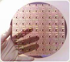
Processed Si wafer supplied by SEMATECH bonded to a glass wafer after all the silicon was removed in the FC-NY, RPI. Prof. James Lu holds the 8" 3D-wafer. Photo by Russ Kraft.
Based on a 1965 prediction by Gordon E. Moore, who later co-founded Intel, the maxim says that the processing power of integrated circuits will double every 18 months. Moore’s Law remains a cornerstone of the semiconductor industry, but researchers at Rensselaer say that foundation will soon crumble unless manufacturers make some radical changes — in a new dimension.
“Fundamentally, we are at a crossroads and new technologies need to be seriously looked at,” says Dr. Om Nalamasu, director of the Center for Integrated Electronics and recently appointed as vice president of research at Rensselaer. What Nalamasu refers to is sustaining the production of smaller, faster, and cheaper chips. “The idea is to make things small, but still with productivity enhancements of 30 percent year to year,” he continues, pointing out that as chips get smaller and smaller, the cost of fabricating them goes up dramatically. “By 2010, you would be using 45 nanometer design rules, and by one estimate a fabrication facility would cost $10 billion.”
But cost is not the only challenge facing chip manufacturers, according to Jian-Qiang “James” Lu, an associate research professor of physics and electrical engineering at Rensselaer. Indeed, chips of the 1960s were flat wafers that held a few dozen transistors, or junctions for electrical signals, connected by wires. Today’s integrated circuits are still flat chips, but now the size of a fingertip and containing hundreds of millions of transistors. Lu believes that if chip makers continue to cram more transistors onto smaller flat chips, Moore’s Law will soon be broken, and chip manufacturers will no longer be able to create better performing chips at the same pace.
“When you make a chip smaller, the wires connecting the transistors also become thinner and closer,” says Lu, explaining that the wires will now have higher impedance and heat up more, thus causing signal delays, and ultimately limiting the processing speed.
“Now the chip is smaller and the cost of a single transistor is cheaper, but it’s not faster anymore because it gets hotter.” Another factor that slows processing speed is the length of the wires that interconnect the transistors. As Lu describes, a “global” interconnect wire might stretch diagonally from one corner of a chip to another. “The global interconnect dominates the speed,” says Lu, adding that the longer the wire, the slower a signal travels from one transistor to another. In an industry with a great need for speed, every nanosecond counts.
Kathryn Guarini, a manager of research at IBM, agrees with Lu’s assessment. “We’re approaching some fundamental physical limitations that don’t allow us to use the same scaling routines of shrinking every dimension of the transistor while achieving requisite performance enhancement,” she says. “Every year we can go and buy a faster laptop; that trend can’t continue forever with the technology we have now.”

A New Dimension
Just as civil engineers of the 1880s began building skyscrapers in crowded cities, Lu is pioneering chip real estate by developing high-rise, 3-D chips to alleviate congestion in integrated circuits. Lu says that stacking chip layers means transistors don’t have to be on opposite corners of a chip. Instead, those same two transistors can be very close, one above the other. “Make the interconnect wire shorter, and you cut the delay time,” says Lu. “A simple way to make them shorter is to stack the transistors.”
The notion of stacking chip layers has been around since the 1980s. Some companies today “package” whole chips layered one on top of another. But Lu’s high-rises are different because they involve just one base layer of silicon with active wafers layered on top. “We call that monolithic because all the processing is done at the wafer level,” says Lu. “We can connect two chips anywhere with really short interconnect wires that can be just a few microns.”

Wafer-level stacking also allows for short connections between different types of chips. “Particularly today the industry is trying to combine memory with the processor, and more than half of the chip is taken up by memory,” Lu explains. “When we stack layers, we have a processor on the bottom and layer the memory on top, with a short access time between them.” Lu says the reduction of memory access time would be a huge advancement for large-scale computer clusters calculating nuclear reactions and weather broadcasting, for example.
“You are also creating new functionality,” says Nalamasu. “Such technology has vast implications, for example, integrating biochips with silicon chips. The wonderful thing is that if we adopt this technology, we’ll develop things we can’t even envision today.”
Guarini agrees that 3-D chips look like a promising way to keep integrated circuit development flowing, instead of getting stuck in an industrywide eddy. In fact, she began working on 3-D chip research, part of which involved collaboration between IBM and Rensselaer. “Three-D integration is a hot topic because of all the challenges facing the semiconductor industry with the traditional approaches to promoting circuit performance,” she says. “By three-D integration, we’re envisioning processes that allow the use of two or more layers of transistors connected together and communicating one layer to another. That gives you more potential opportunities for changing the way that these chips perform.”
Rensselaer at the Helm
Lu first started speaking about 3-D chips at industry conferences in 1999, and even then industry leaders thought the concept was intriguing. To date, Lu and his colleagues have published roughly 70 papers on the subject and have three patents pending. Yet there’s still much work to be done. Lu is busy speaking at conferences, developing prototypes, running simulation models, and investigating fabrication techniques as close to the current techniques as possible to avoid enormous manufacturing costs.
According to Guarini, “with any new technology, part of the challenge is proving its manufacturability and reliability, as well as a true demonstration of its advantages. There’s still a bit of work need to make the technical and business case for such a large-scale investment.”
Rensselaer is leading the way to that next phase and next dimension. “Our idea is to develop three-D technology to a point that companies would be willing to say ‘this is a technology that I can take a much closer look at for incorporating into manufacturing,’ ”Nalamasu explains.
Rensselaer is working with IBM through a government grant, and also has collaborations with other technology companies including Sematech and Freescale semiconductor. Both Lu and Nalamasu say they are working to form a consortium of industrial, military, and government partners to accelerate the development of 3-D chips at this crucial juncture for the industry. “Right now is the critical time to commercialize this process because there aren’t a lot of options out there,” say Lu. From his perspective, things are looking up.
Source: Rensselaer Polytechnic Institute (By Karen DeSeve)


